
Knowledge Hub
One content hub for visible progress and evergreen buying knowledge
This hub combines two things: dated updates that show current execution activity, and evergreen guides that answer recurring engineering and sourcing questions without getting stale after a week.
Last reviewed
September 26, 2026
Published guides
50
Covered topics
64
Recently Updated
Guides refreshed most recently
Every article below carries a visible last-reviewed date, so you can tell whether the node, packaging and cost guidance still reflects current foundry practice.
ISSCC: What It Is, What Happened in 2026, and How Teams Actually Use It
A working reference to the International Solid-State Circuits Conference — the verified 2026 edition in detail, tentative future dates, and how a design or sourcing team should read the programme without confusing published papers with production-ready IP.
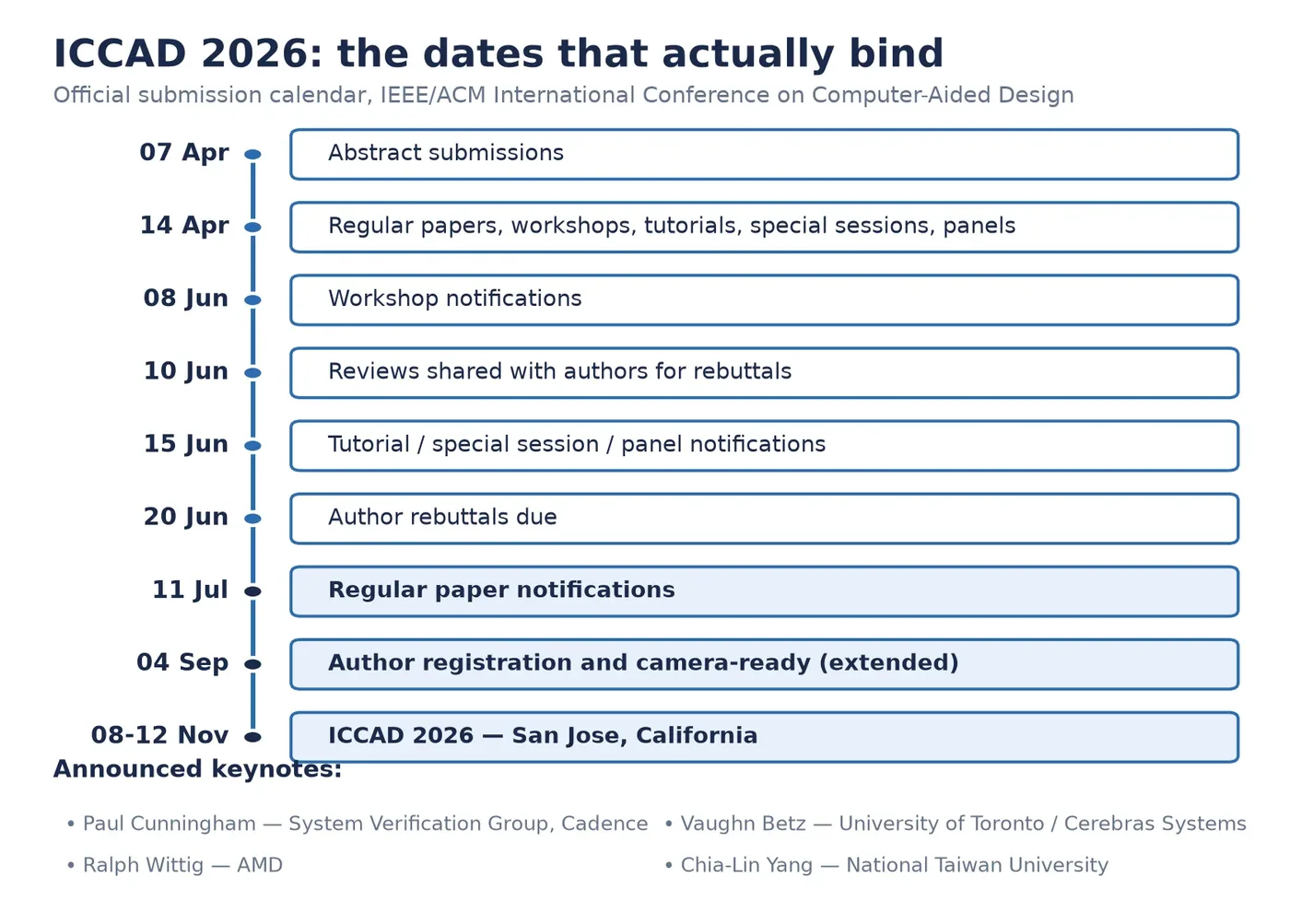
ICCAD 2026: Verified Dates, Keynotes and How an EDA Conference Reads for a Chip Team
A working reference to IEEE/ACM ICCAD — the verified 2026 dates and submission calendar, the four announced keynotes, what the call for papers covers, and how a chip team should read an EDA conference without confusing a paper with a production flow.

Inside ISSCC 2023–2026: Scenes from the Main Stage, the Sessions and the Expo Floor
An original photo walk through the last four ISSCC editions — plenary stages from 2024 to 2026, the Pederson Award ceremonies, the Student Research Preview, session rooms at full scale and the composition of the exhibition floor.
Evergreen Guides
Guides for decisions you make before tape-out
These pages target durable questions such as when to use MPW, how to choose a node and what to prepare in packaging or test before tape-out.
What Is MPW Service and When Should a Chip Team Use It?
A practical primer on MPW shuttle service, who it fits, how it lowers mask cost and where it sits in the broader tape-out path.
How to Choose the Right Foundry Node for an ASIC Program
Node choice is not only about shrinking geometry. It is a trade-off across cost, IP ecosystem, power, packaging and business timing.
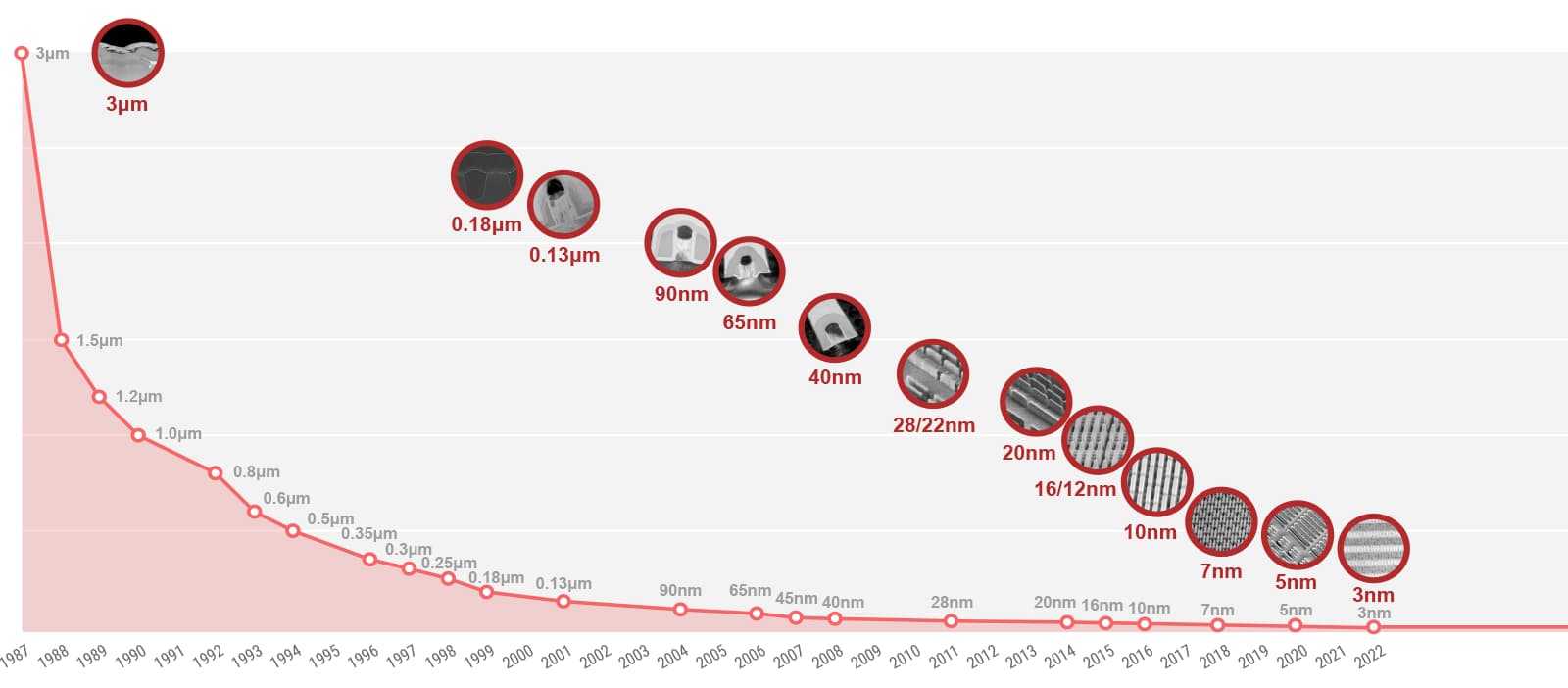
IP Fit Planning Before Tape-Out: A Checklist for ASIC Teams
IP choice is more than a licensing problem. This checklist walks through the four IP categories to settle first, license constraints, foundry qualification and the cost of last-minute changes.
Packaging and Test Checklist to Prepare Before Tape-Out
Packaging and test are where many programs lose momentum. This checklist explains what should be aligned before wafers come back.
MPW vs Full Mask: Which Tape-Out Path Should You Choose?
MPW and full mask solve different problems. This comparison explains the cost, lead-time, volume and risk trade-offs so the right path is chosen early.
Process Node Comparison: From 180nm to 5nm and How to Choose
Node choice is not a single ladder. Mature and advanced nodes serve different products, costs and ecosystems across the 180nm to 5nm range.
Process Technology Comparison: CMOS, BCD, BiCMOS, RF and FinFET
Beyond node size, the type of process technology decides what a chip can do. Compare CMOS, BCD, BiCMOS, RF and FinFET by function.
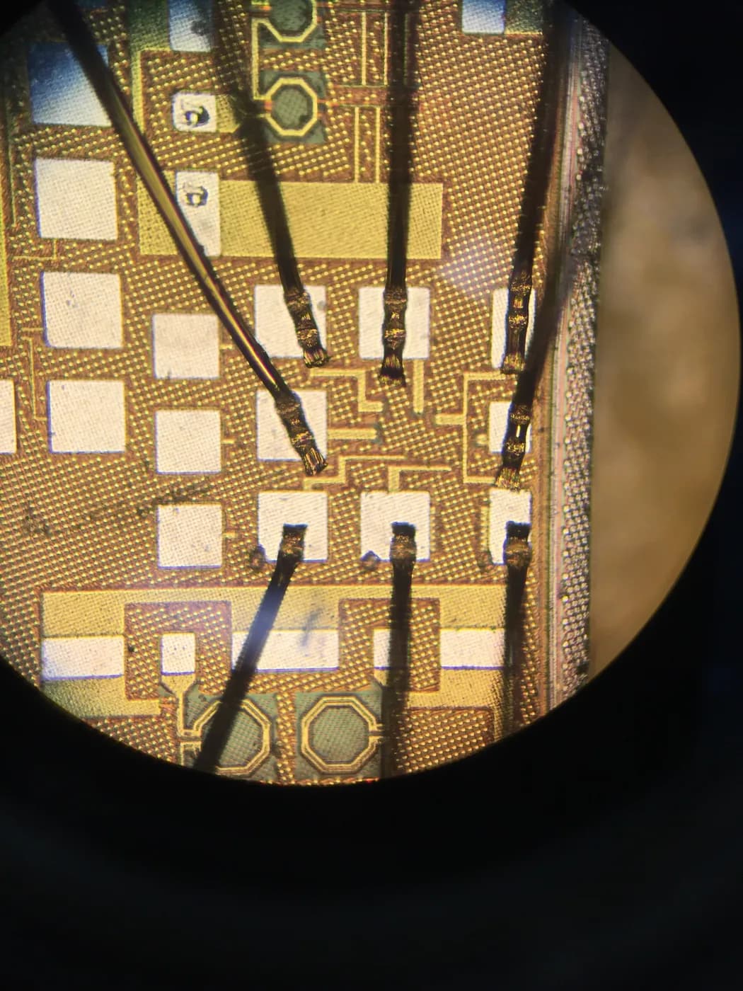
Foundry MPW Node Comparison: TSMC, SMIC, UMC and More
Each foundry offers MPW shuttle services at different nodes with different schedules, costs and access conditions. This comparison maps the landscape.
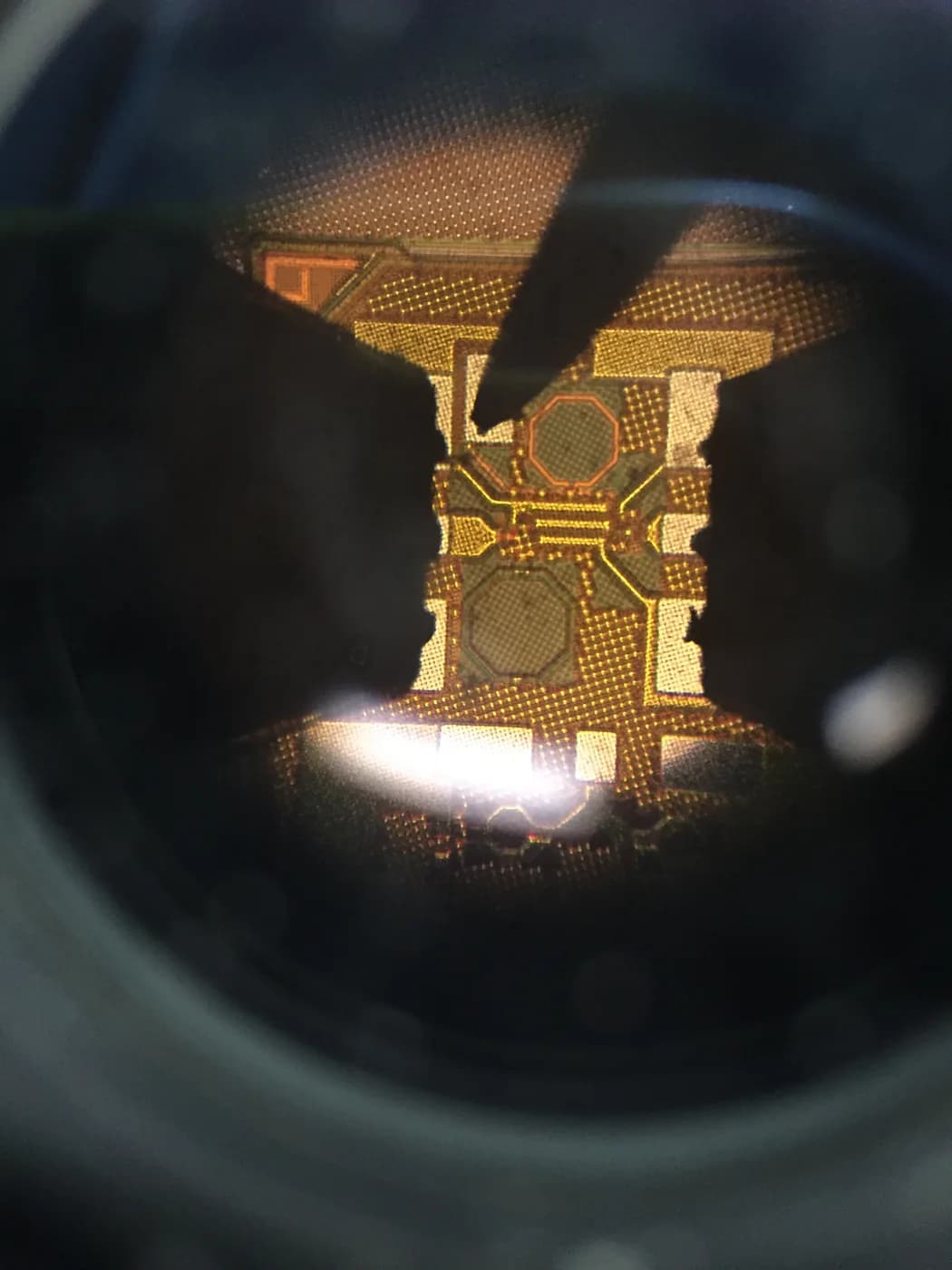
What We Learned Taping Out a 28nm Computing-in-Memory Chip
A field note from a real 28nm CIM tape-out: how the backend flow was structured, what surprised us, and the three decisions that protected the schedule.
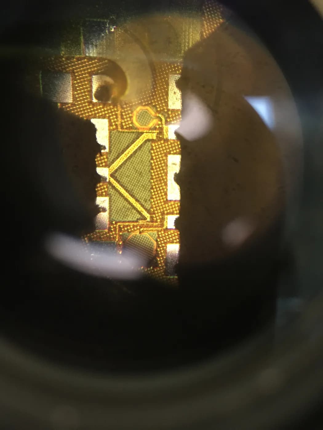
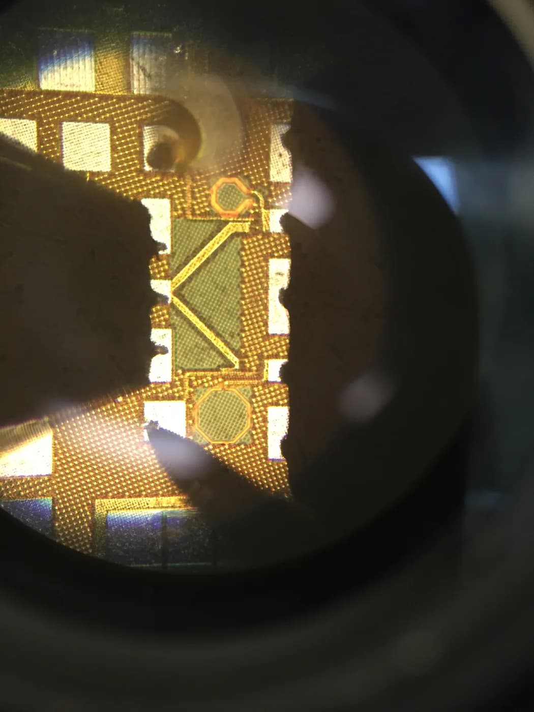
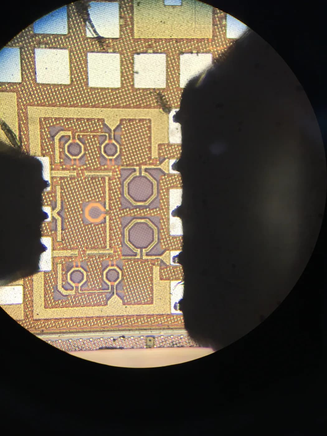
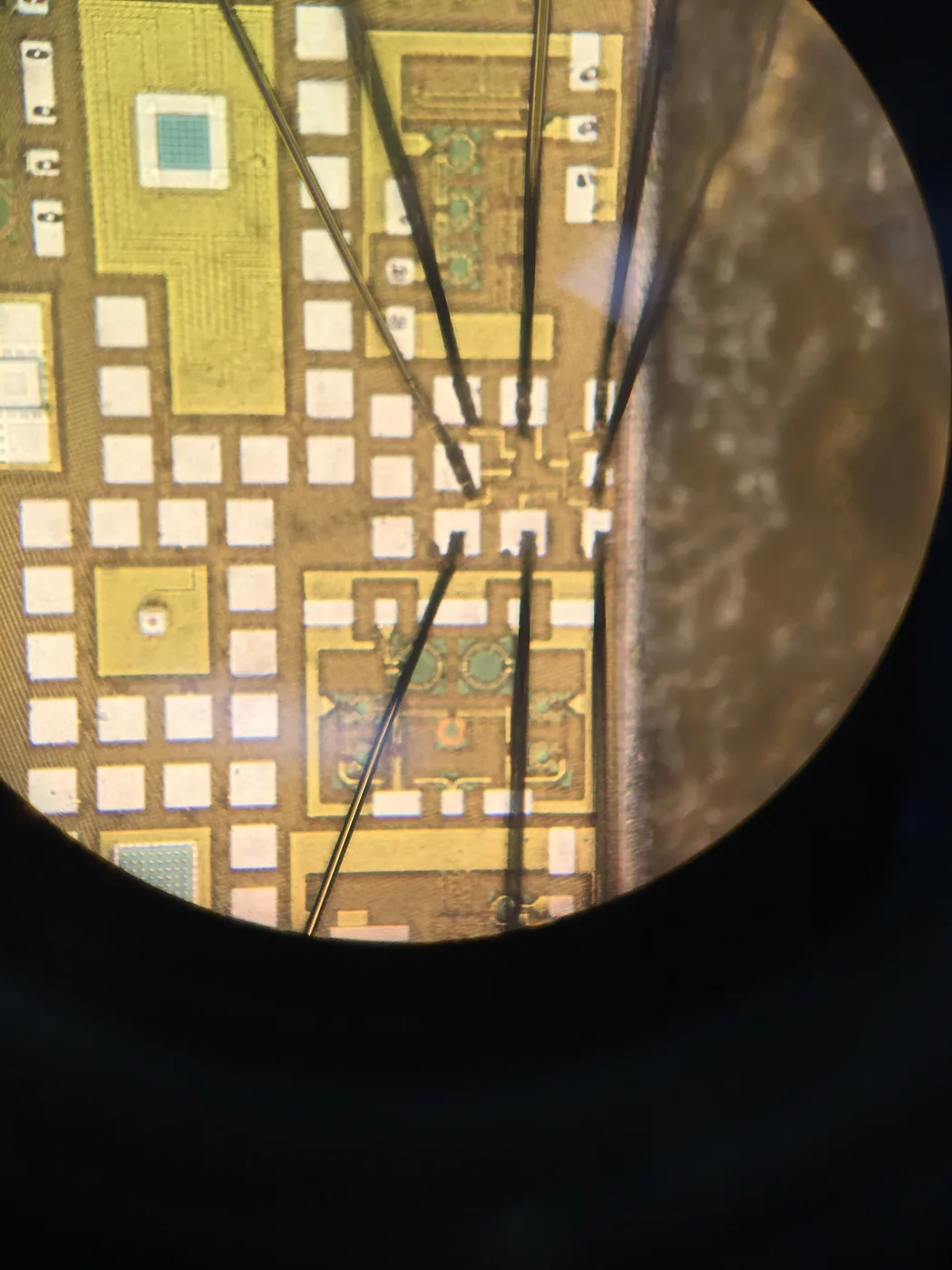
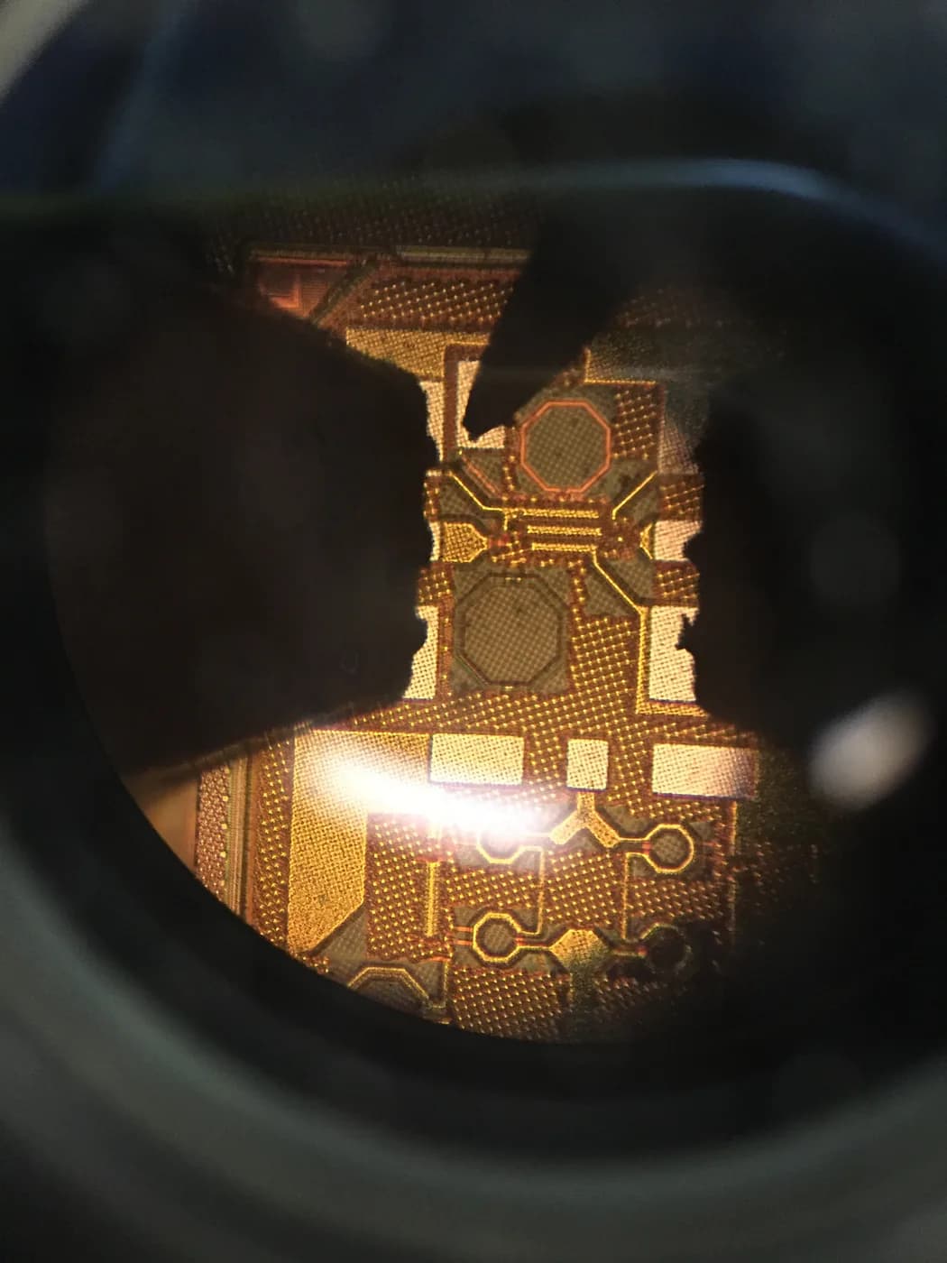
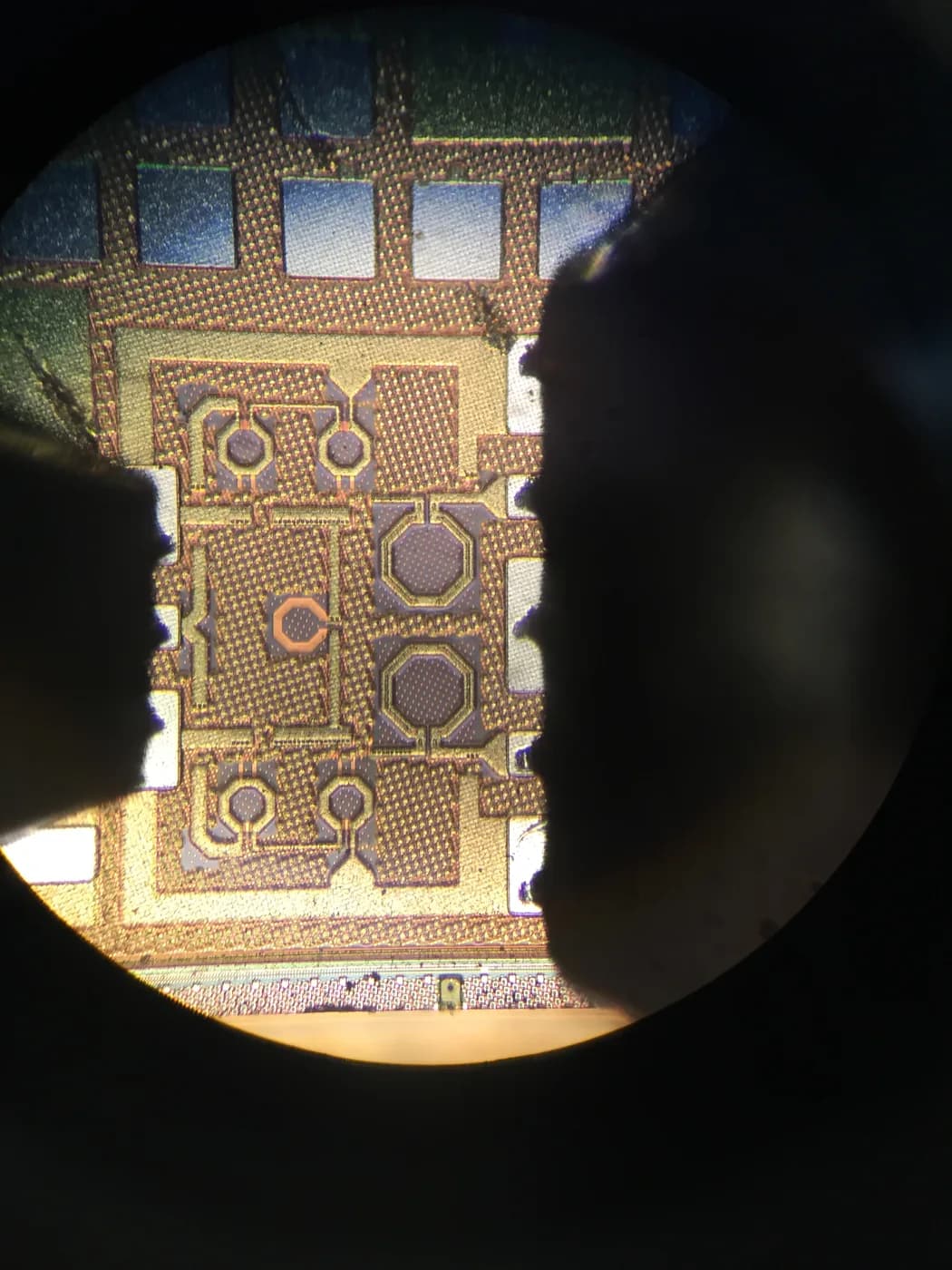
RF-SOI LNA: Three Tape-Outs in One Year
How a small RF fabless team ran three MPW shuttles for an LNA and RF switch in a single year — and what the die photography was used for.
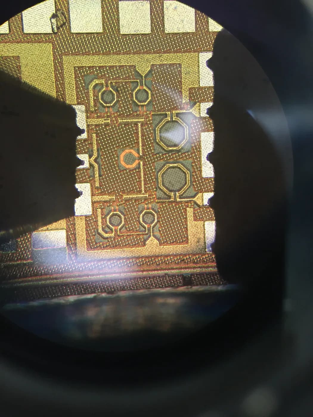
Dual-Node TSMC CyberShuttle Enrollment for an Automotive MCU
A walkthrough of enrolling one automotive MCU program into TSMC CyberShuttle at two nodes simultaneously, and the AEC-Q100 prep that ran alongside it.
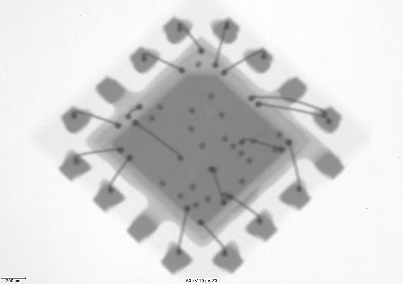
How to Select the Right IC Package: QFN, BGA, WLCSP, Flip-Chip and SiP
Package choice is a pre-tape-out decision that drives board cost, thermal, RF and yield. A practical framework for matching QFN, BGA, WLCSP, Flip-Chip and SiP to your design.
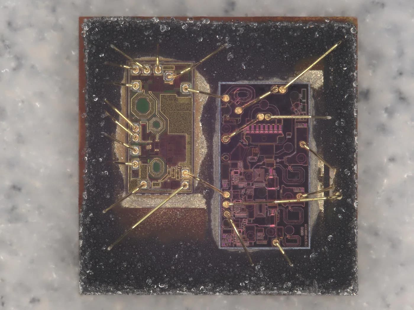
Wire Bond vs Flip-Chip: When Each Interconnect Wins
Wire bonding and flip-chip solve different interconnect problems. Compare cost, electrical, thermal and yield trade-offs to pick the right die-attach for your package.
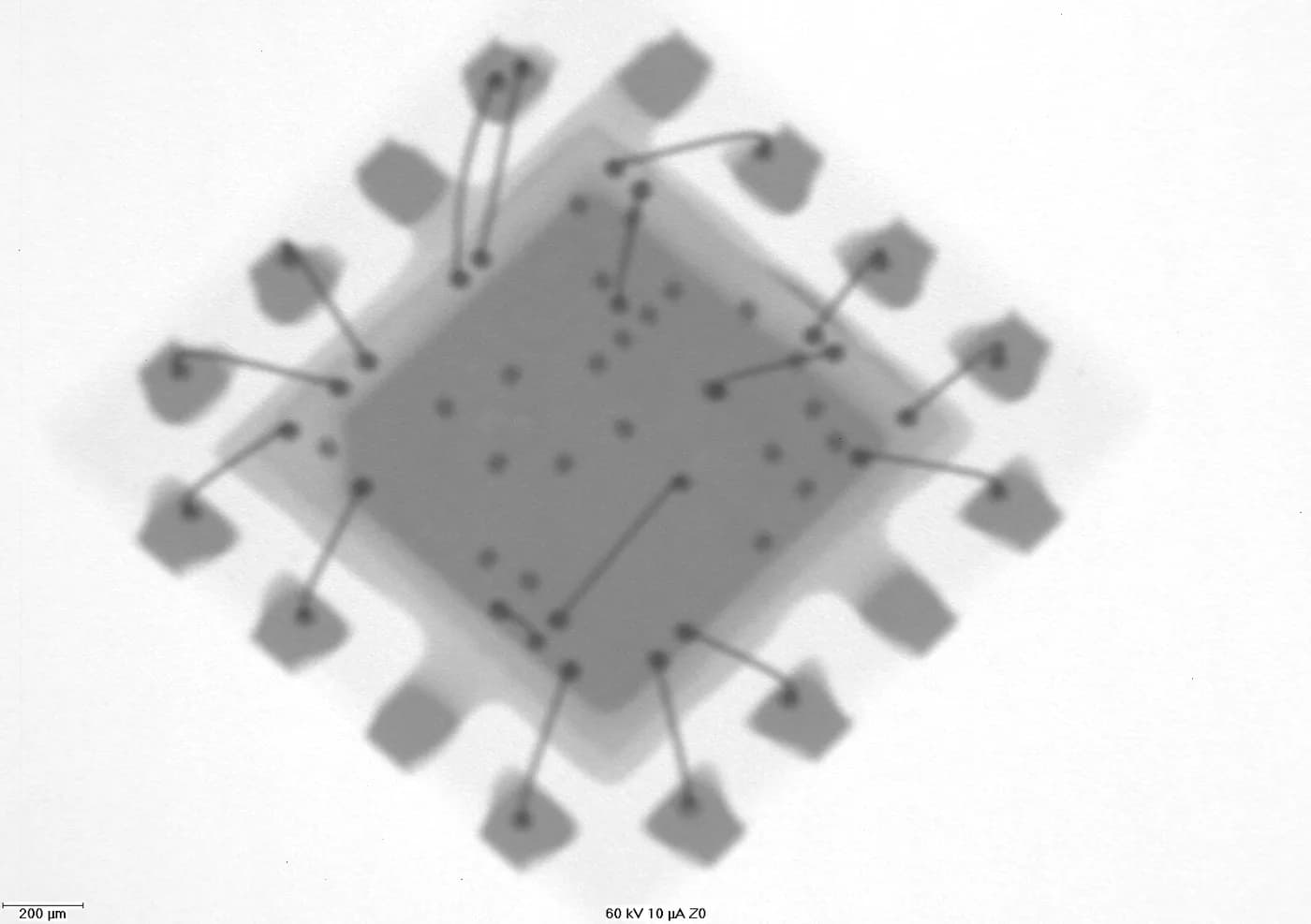
Advanced Packaging and Chiplets: What Changes for ASIC Programs
Chiplets and advanced packaging shift integration from the wafer to the package. Understand 2.5D, 3D, SiP and heterogenous integration, and when they beat a monolithic die.
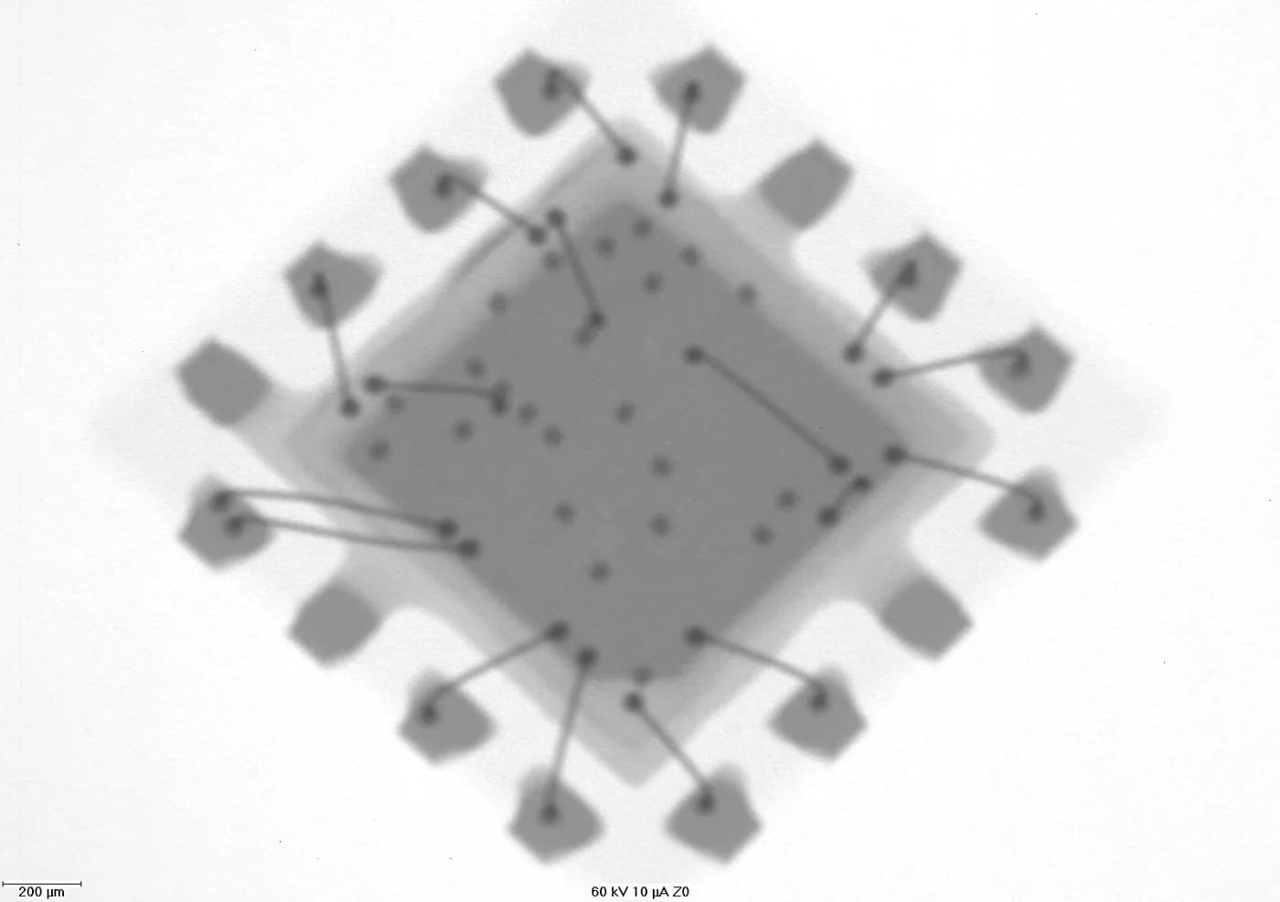
Packaging SiC and GaN Power Devices: What Is Different
Wide-bandgap SiC and GaN power devices stress packages in ways silicon does not. Compare thermal, parasitic, gate-drive and qualification needs for power packaging.
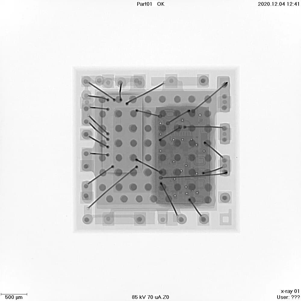
Reducing Test Cost: DFT, Yield and ATE Strategy
Test cost is paid on every die, good or bad. Learn how design-for-test, yield learning and ATE strategy cut cost per good unit without shipping risk.
Wafer Sort (CP) vs Final Test (FT): What Each One Catches
Circuit probe and final test are not redundant. Learn what wafer sort catches cheaply, what only final test can see, and how to split coverage between them.
ATE Time, Probe Cards and Load Boards: Where Test Cost Really Goes
Test cost is usually quoted as a per-hour tester rate. The real drivers are test time, tester class and the NRE of probe cards and load boards.
DFT Basics: Scan, BIST and JTAG for ASIC Teams
Design for test is decided before tape-out, not after wafer return. A plain-language guide to scan, compression, BIST and boundary scan.
Reliability Qualification: HTOL, ESD and AEC-Q100 Explained
What qualification actually proves, which stresses are standard, and when a part genuinely needs AEC-Q100 versus a lighter qualification plan.
Burn-In and System-Level Test: When They Pay For Themselves
Burn-in and SLT are expensive insertions. Learn which failure modes justify them and which programs should skip both.
DPPM Targets and Yield: Setting Test Escape Limits That Make Sense
DPPM is a business decision dressed up as a test metric. How to set a defensible target and what it costs to hit it.
Soft, Firm and Hard IP: How to Choose for an ASIC Program
The same function can arrive as RTL, as a placed netlist, or as a hardened macro. Each has a different cost, risk and schedule profile.
IP Licensing Models Explained: Upfront, Royalty, Subscription and Escrow
What you actually pay for an IP core, how per-die royalties behave at volume, and which contract terms decide whether a deal is good twelve months later.
The IP Vendor Landscape: Who Sells What, and How to Shortlist
Foundry IP programmes, large EDA vendors, processor specialists and the open-source ecosystem each solve a different problem. A practical way to shortlist.
Arm vs RISC-V for an ASIC: How the Decision Actually Gets Made
The architecture debate is usually settled by software ecosystem and qualification evidence, not by the instruction set. What to weigh for a real program.
IP Integration Pitfalls: CDC, UPF, Timing and the Late ECO
Most IP problems are not in the core. They are in clock domain crossing, power intent, interface timing and the ECO that arrives two weeks before tape-out.
IC Package Thermal Management: What Actually Moves Junction Temperature
Thermal resistance is a system property, not a package property. What board design, TIM and airflow do to the number on the datasheet.
Package Substrates, Materials and MSL: What Buyers Should Ask
Substrate type, mold compound and moisture sensitivity determine cost, reliability and how you have to handle parts on the line.
Packaging Cost Drivers and Lead Times: Planning the Part Everyone Forgets
Assembly is often quoted late and underestimated. What actually drives package cost and where the weeks go.
What Actually Changed in Advanced Packaging for 2026 Programmes
A grounded read on the 2026 advanced packaging landscape — 2.5D and 3D capacity, fan-out moving down-market, glass substrates entering pilot lines, and optics arriving in the package — and what each one does to cost, lead time and risk.
Foundry Process Updates in 2026: What Changed, and What It Does to Node Choice
A sourcing-focused read on 2026 foundry developments — where Chinese capacity went, why BCD and power got busy, and how memory and heterogeneous integration are pulling ordinary programmes toward package-level decisions.
VeriSilicon in 2026: What the SiPaaS Numbers Actually Say
A read on China's largest semiconductor IP and design-service vendor using its own 2026 filings — how the licensing-to-mass-production mix shifts, what 77% IP gross margin really implies, and where this model helps or hurts an outsourced programme.
ISSCC: What It Is, What Happened in 2026, and How Teams Actually Use It
A working reference to the International Solid-State Circuits Conference — the verified 2026 edition in detail, tentative future dates, and how a design or sourcing team should read the programme without confusing published papers with production-ready IP.
Synopsys in FY2026 Q3: What the Numbers Say About EDA and IP Supply
Reading Synopsys' reported third-quarter fiscal 2026 results as supply-chain intelligence — segment split, the Ansys effect, divestitures, and the export-control caveat sitting inside the guidance.
Cadence in 2026: Record Backlog, IP Growth Above 40%, and Agentic AI
Cadence's reported 2026 results read for what they say about IP supply, advanced packaging tool flows and where agentic AI is actually being deployed — with the specific interfaces driving demand named.
ICCAD 2026: Verified Dates, Keynotes and How an EDA Conference Reads for a Chip Team
A working reference to IEEE/ACM ICCAD — the verified 2026 dates and submission calendar, the four announced keynotes, what the call for papers covers, and how a chip team should read an EDA conference without confusing a paper with a production flow.
Inside ISSCC 2023–2026: Scenes from the Main Stage, the Sessions and the Expo Floor
An original photo walk through the last four ISSCC editions — plenary stages from 2024 to 2026, the Pederson Award ceremonies, the Student Research Preview, session rooms at full scale and the composition of the exhibition floor.
ISSCC 2026 in Numbers: Record Submissions, and What China's Fourth Consecutive Year at the Top Actually Shows
A data read on the 73rd ISSCC using the conference's own report and Chinese-language coverage of the results — submissions, acceptance, regional split, institutional leaders, and the future-technology track where China appeared for the first time.
JCET, TFME and Huatian: What Each of China's Three Packaging Houses Is Actually Good At
A capability comparison of the three mainland OSATs that carry most domestic advanced packaging — technology platforms, base specialisation, and customer concentration — plus which share figures can and cannot be relied on.
Imagination's E-Series: GPU IP That Runs Graphics and AI on the Same Core
What Imagination's E-Series actually specifies — matrix acceleration inside the shading cluster, published throughput figures, supported precision formats — and what the strategy shift behind it means for anyone licensing GPU IP.
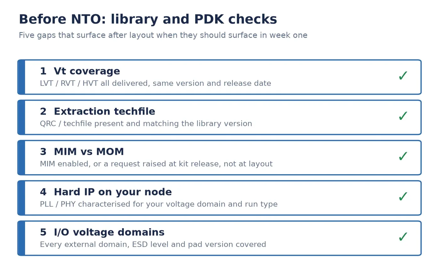
Case Study: The Library and PDK Gaps Found Before a SMIC 40LL Tape-Out
Three concrete gaps surfaced on a SMIC 40LL program during NTO preparation: a missing parasitic extraction techfile, a PDK shipping only MOM capacitors, and unclear commercial terms for the node's PLL. What each costs if found late.
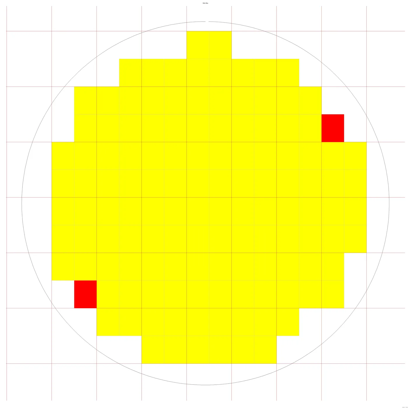
Case Study: 12.24 × 15.24 mm Die on 200 mm Places 127 Dies — What the Map Says
A real 200 mm wafer map for a 12.24 × 15.24 mm die places 127 gross dies. The common closed-form estimate returns 136 for the same inputs. Why the 7% gap exists, and what it means for cost models built on the formula.
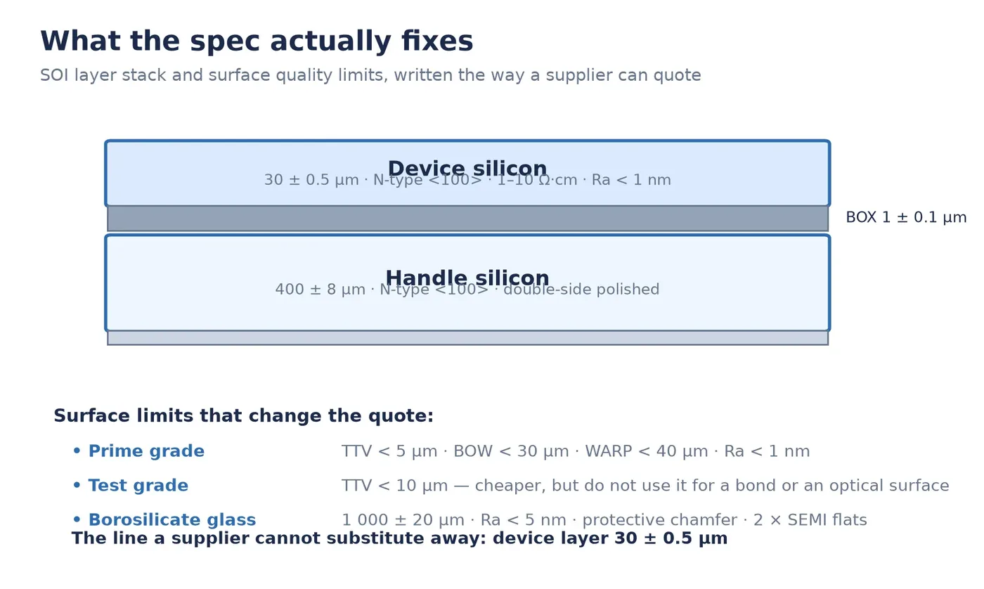
Case Study: Writing a Substrate Spec a Supplier Can Quote — Silicon, SOI and Glass
A real inquiry covering 6-inch prime and test wafers, a 6-inch SOI stack for a pressure sensor, and borosilicate glass. What each line of the spec fixes, and why the SOI device-layer tolerance is the one a supplier cannot substitute away.
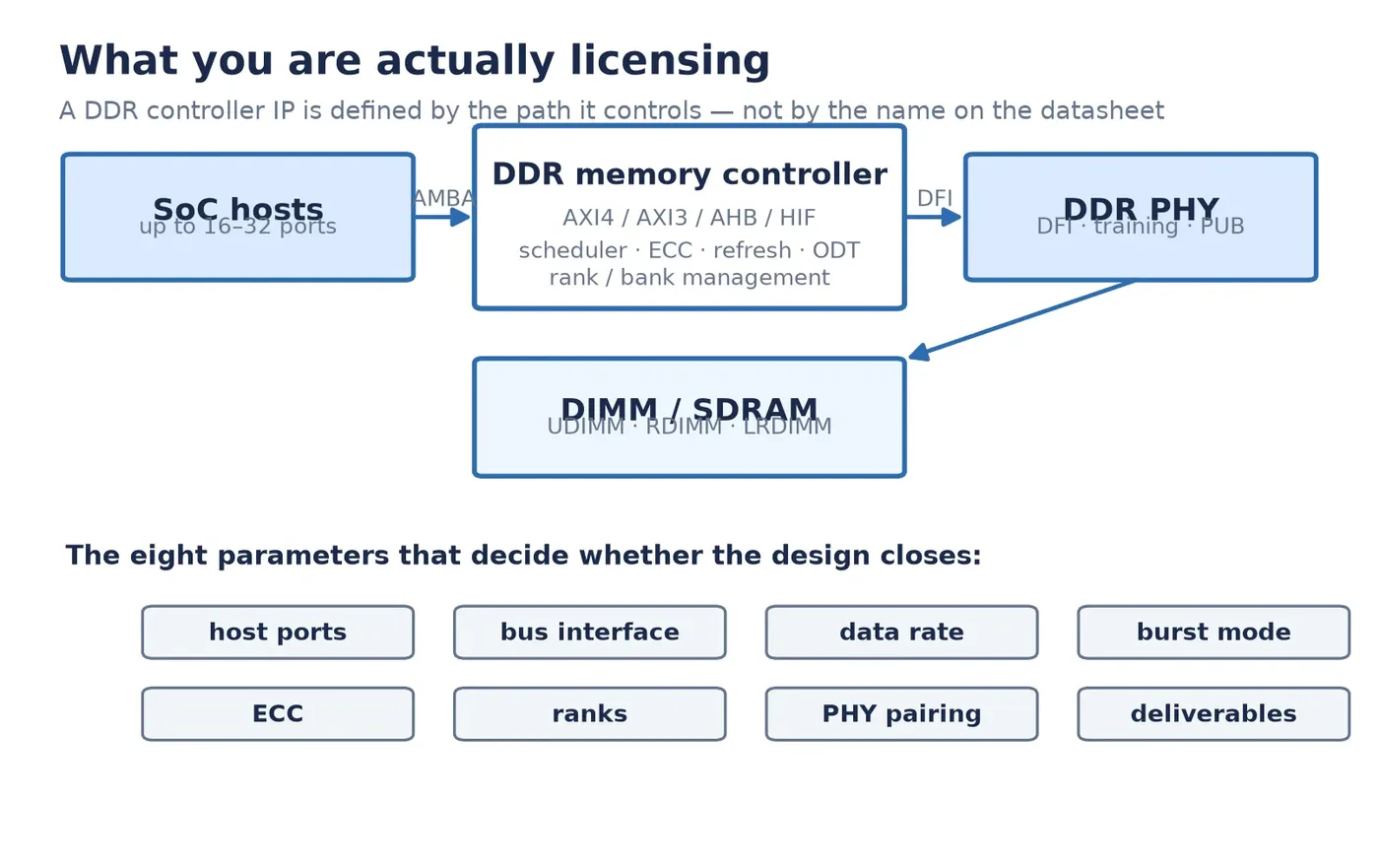
Case Study: Selecting a DDR Controller IP for SMIC 40LL — the Parameters That Decided It
A real selection between two DDR controller IP datasheets for a SMIC 40LL program: host port counts, bus interfaces, burst handling, ECC, DIMM support and what each vendor actually delivers. One was licensed.
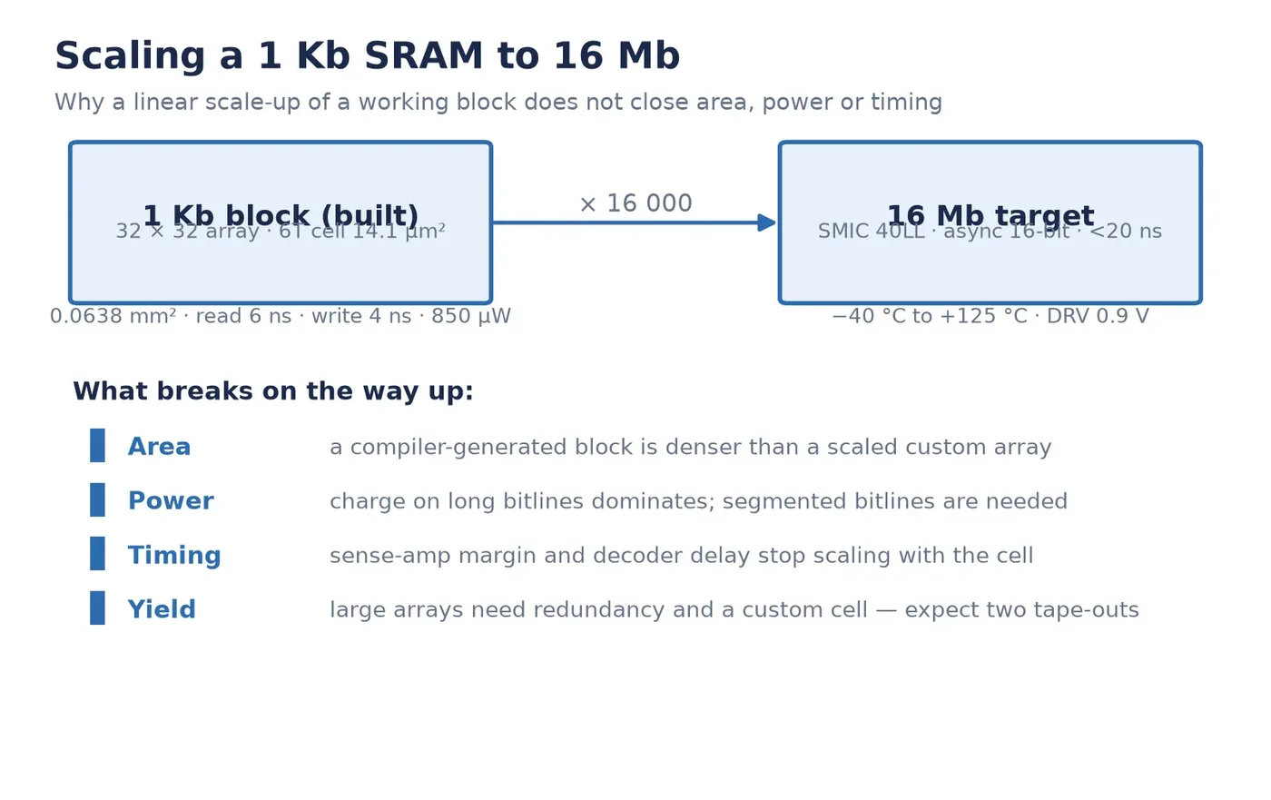
Case Study: Scaling a Working 1 Kb SRAM to 16 Mb on SMIC 40LL
A team had a functional 6T SRAM block on 130 nm and needed 16 Mb on 40LL. Measured sub-block data, why linear scale-up does not close area or timing, and the yield risk that makes two tape-outs the realistic plan.
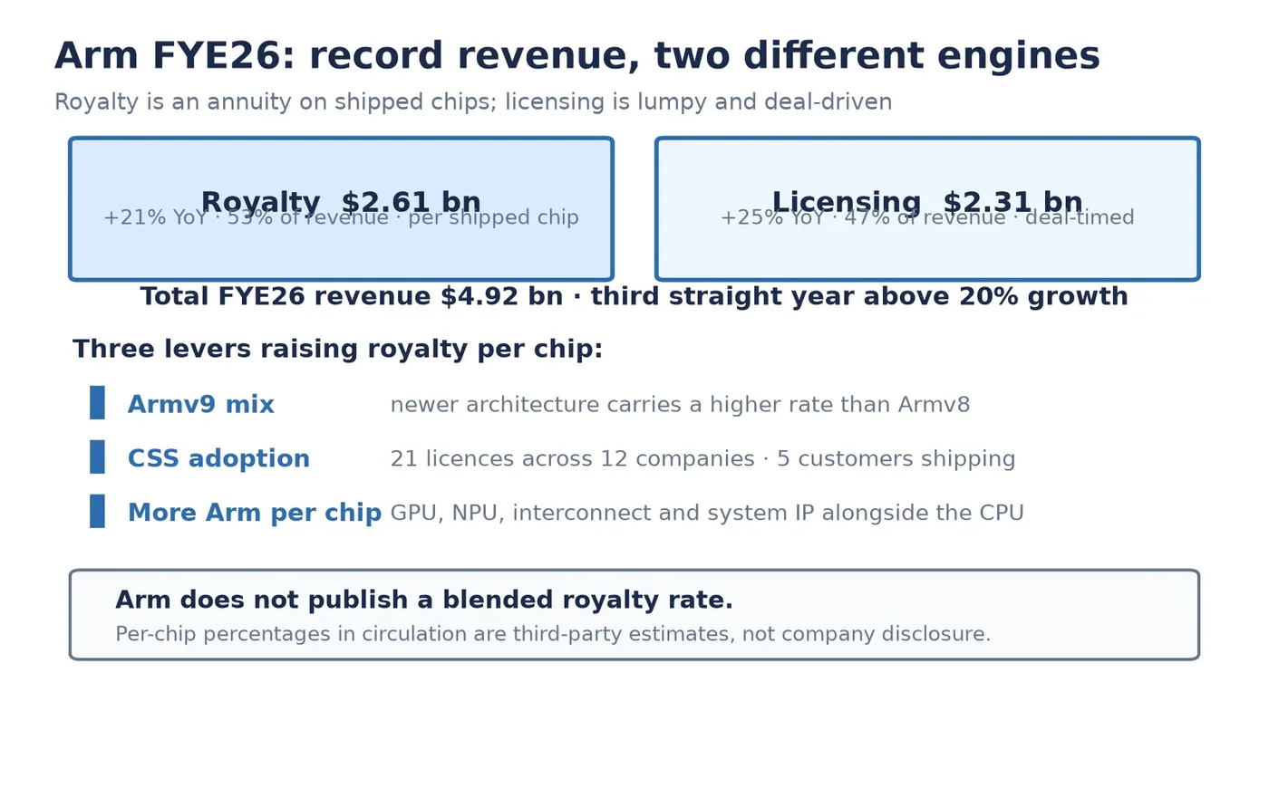
Arm in FYE26: Record Revenue, and the Two Engines Behind It
What Arm's own fiscal 2026 filings and shareholder letters say — record revenue and royalty, the Compute Subsystems shift, roughly half of hyperscaler CPU share, and the decision to sell its own data-centre silicon.
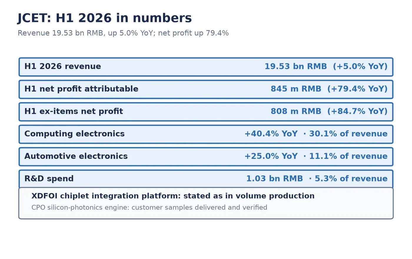
JCET in H1 2026: What the Half-Year Report Actually Says About Capability
JCET's H1 2026 results read as a mix-shift story, not a volume story: revenue up 5%, profit up 79%, computing electronics overtaking everything else. What that means for which programmes the line is actually tuned for.
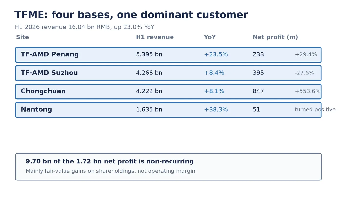
TFME in H1 2026: Four Bases, One Customer, and a Profit Line to Read Carefully
TFME's H1 2026 report shows revenue up 23% and attributable profit up 317% — but most of the profit increase is non-recurring. What the four production bases each do, and how the AMD concentration shapes what you can actually book.
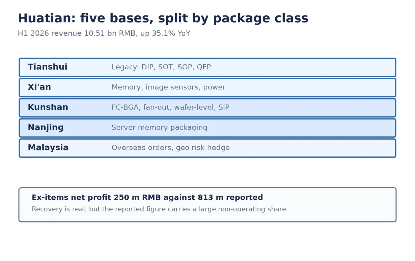
Huatian in H1 2026: The Fastest Growth of the Three, and the Thinnest Profit Line
Huatian grew revenue 35% in H1 2026 — faster than either of the larger two — with profit up 259%. But ex-items profit was 250 million against 813 million reported. What the five-base network actually carries.