
About TOMPW Service
A China-based execution partner for global chip programs
Semiconductor teams worldwide that want one execution-facing partner in Asia instead of managing every foundry, package and test handoff alone.
Operating Model
One execution path
Customers do not have to build a vendor maze from scratch. TOMPW can coordinate the commercial and operational handoff across the silicon delivery chain.
Operating Model
Global communication
The operating model is especially useful for international customers who need predictable English-language coordination around Asia-based manufacturing.
Operating Model
Practical scope control
Projects can start small with MPW or one service line, then expand into package, test, board or turnkey support as the program matures.
Coverage Snapshot
Engineering and delivery capabilities
- Standard process coverage highlighted in current source material spans 12nm to 3um.
- Below-7nm programs are evaluated case by case based on ecosystem fit, schedule and commercial model.
- Common platform references include CMOS, BCD, SOI, SiGe, GaAs, GaN, silicon photonics and MEMS.
Foundry and technology coverage
Visual trust signals for the global main site

























Positioning
Built for cross-border semiconductor execution
That means the content answers practical engineering and sourcing questions, not just a generic company profile. The site lays out service scope, downstream dependencies, packaging and test realities, and article pages that walk through real execution decisions teams face before tape-out.
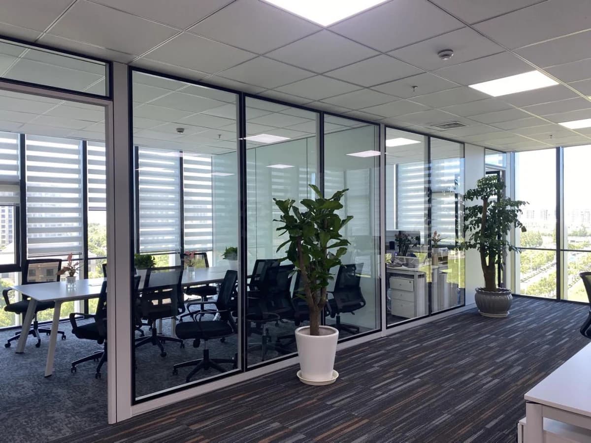
Our Workspace
A hands-on execution team, not a marketing desk
Our team works daily on EDA tools, reviews DRC/LVS results, coordinates shuttle enrollments and tracks wafer delivery across Asia-based foundries.
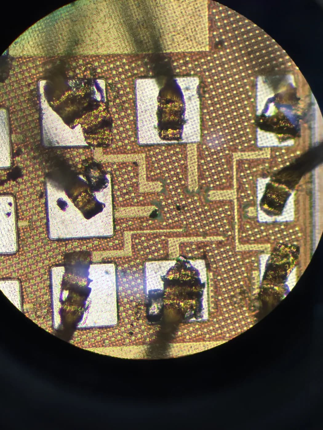
The Team
Engineers who have actually taped out chips
TOMPW has been running tape-out and shuttle programs since 2014 — backend sign-off, analog and RF tape-out, packaging and test. We ship GDSII, not slide decks.
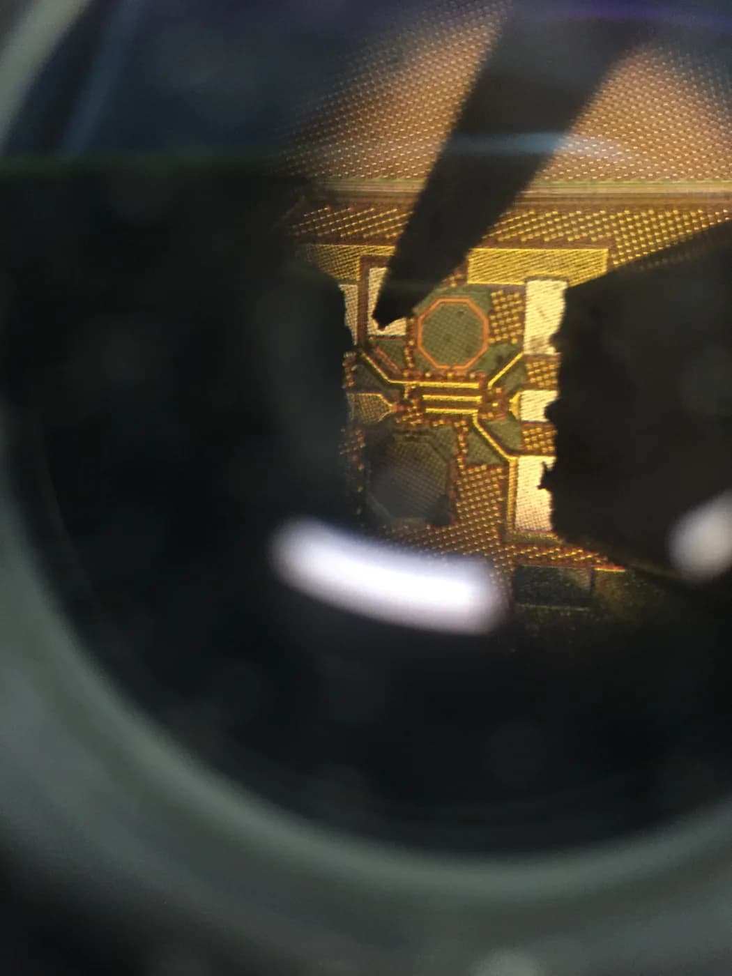
Daily Execution
DRC, LVS and shuttle tracking
Every program is tracked against real EDA sign-off milestones — not status decks.
The Team
Engineers who have shipped silicon at leading companies
TOMPW's execution team blends foundry-access, IP and design expertise earned across global chip programs. The people below lead customer engagements and technical planning.
CEO, TOMPW Service
Henry
Henry is the CEO of TOMPW Service and a chip-design specialist with 20 years in the semiconductor industry. Before building TOMPW he worked on chip programs at Qualcomm, Samsung and Spreadtrum, giving him first-hand exposure to advanced-node and mainstream tape-out across global fabs. He leads TOMPW's foundry-access and ASIC delivery work.
IP & Design Lead, TOMPW Service
Daniel
Daniel spent many years with leading semiconductor IP design houses, focusing on IP selection, integration and hardening for complex ASIC programs. At TOMPW he helps teams choose and integrate third-party IP against the right foundry, node and PDK constraints.
Silicon Engineering Lead, TOMPW Service
Jim
Jim brings many years of silicon-engineering experience from Apple and Broadcom, with deep exposure to high-performance SoC design, verification and production bring-up. At TOMPW he advises teams on design-to-silicon execution across advanced and mainstream nodes.
Selected Engagements
Real projects we have delivered
Below is a sample of actual customer engagements. Client names are withheld; the application, process and outcome are shown at a non-disclosing level.
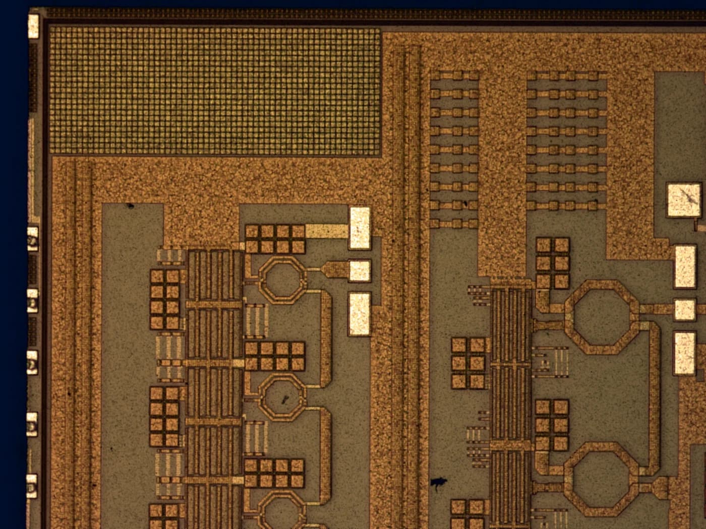
28nm CMOS
University CIM Research Lab
Computing-in-Memory (CIM) chip
Service: Full backend design flow from netlist to GDSII sign-off
First-pass silicon achieved with DRC/LVS clean on target foundry shuttle run.
180nm BCD + MEMS post-process
University Sensor Research Team
Multi-sensor calibration & test system
Service: Sensor characterization, test program development, CP/FT coordination
Delivered calibrated sensor samples within 8 weeks of wafer receipt.
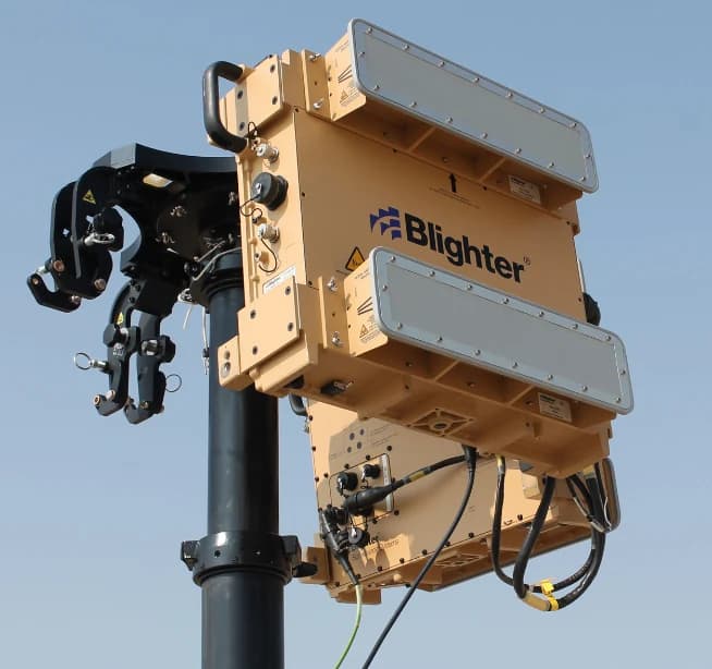
GaN-on-SiC + Ga2O3 (emerging)
Wide-Bandgap Power Device Startup
GaN/Ga2O3 wide-bandgap power device
Service: Process window validation, device characterization benchmark testing
Completed full electrical characterization report used for Series A investor deck.
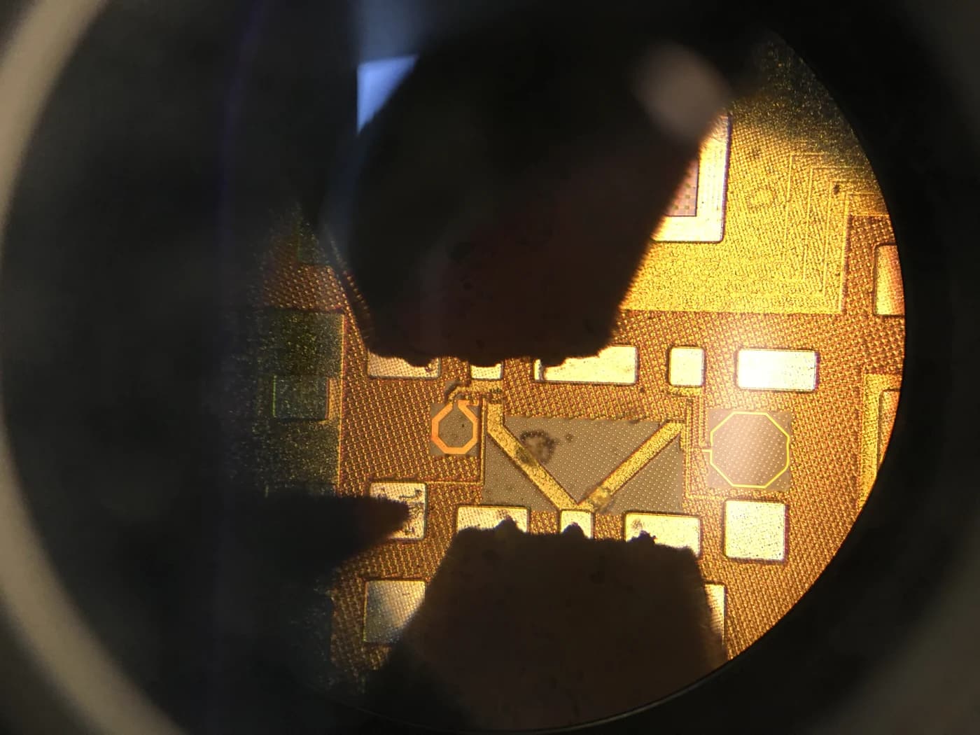
0.18um RF-SOI + SiGe BiCMOS
East China RF Fabless Company
LNA + RF switch transceiver
Service: Tape-out coordination, probe station die photography, package selection
Multiple tape-out runs completed; die photos captured for customer documentation.
0.35um BCD (high voltage)
Shanghai Power IC Startup
High-voltage switch controller
Service: MPW enrollment, mask cost optimization, wafer delivery tracking
Reduced per-run MPW cost by ~30% through multi-foundry shuttle comparison.
40nm automotive + legacy 180nm BCD
Suzhou Automotive Semiconductor Company
Automotive-grade MCU / power management IC
Service: TSMC CyberShuttle enrollment, AEC-Q100 prep consultation, packaging roadmap
Successfully enrolled in TSMC 2024 2H CyberShuttle program for two nodes simultaneously.