
Service Architecture
From first shuttle wafer to delivered product
TOMPW Service is strongest when customers need one execution-facing partner across MPW, NTO, full mask, package, test and downstream productization steps instead of isolated vendors.
Tape-out & Foundry Access
MPW, NTO and full-mask shuttles across 29 partner fabs.
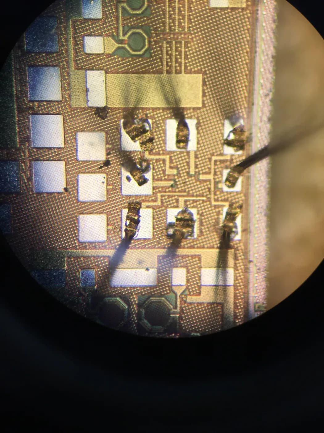
LOWER NRE · FASTER FIRST SILICON
MPW / Fab Shuttle
Compare public shuttle windows across foundries, control first-silicon cost and move from tape-out planning to wafer delivery with one execution path.
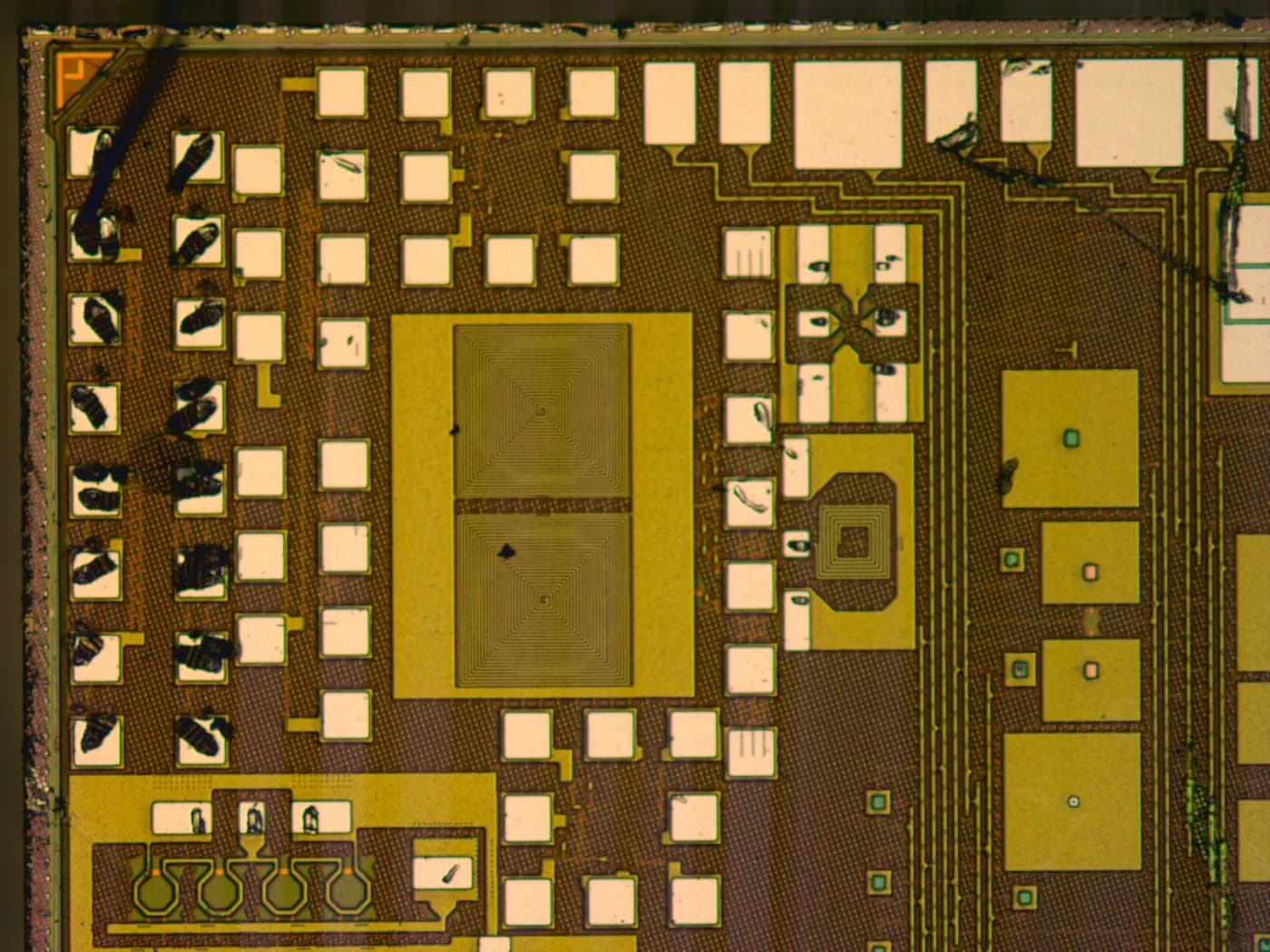
PRODUCTION RAMP · DEDICATED MASK SET
Full Mask / Production Foundry
Move validated designs into dedicated mask production with yield, volume and supply planning support.
Design, IP & Engineering
ASIC/SoC architecture, verification, physical design and licensable IP cores.
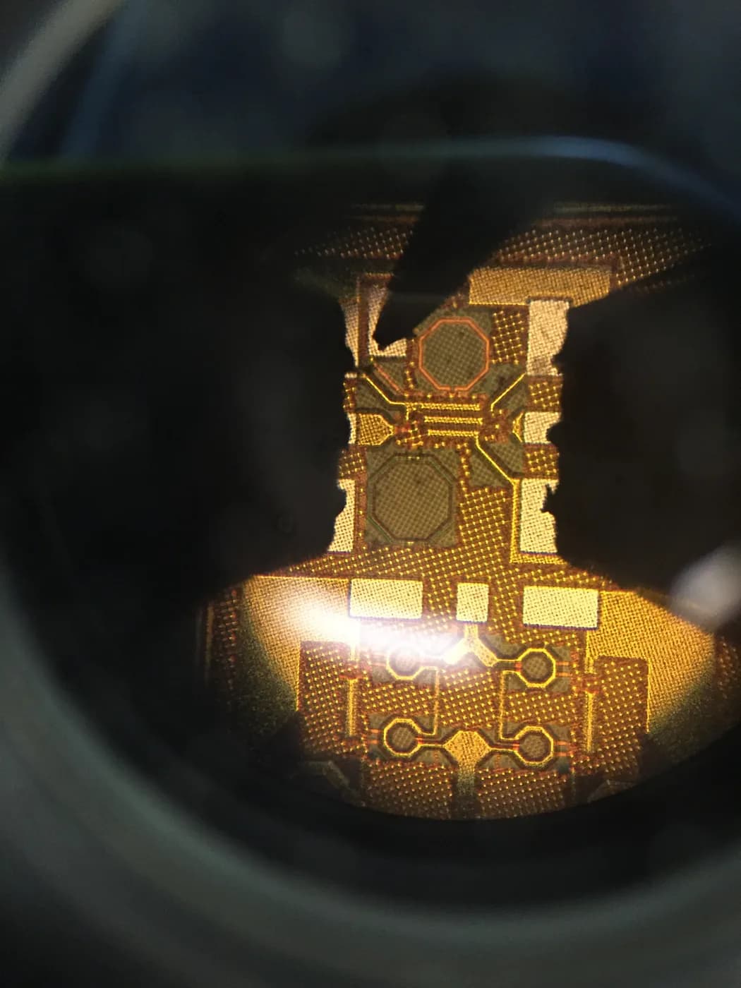
ARCHITECTURE TO RTL
ASIC / SoC Design
Support architecture, RTL and integration planning for teams moving from specification to implementation.
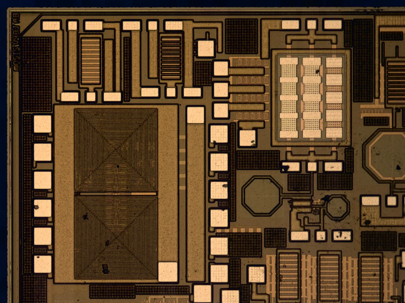
FIRST-SILICON CONFIDENCE
Design Verification
Strengthen first-silicon confidence with structured verification, validation planning and downstream debug preparation.
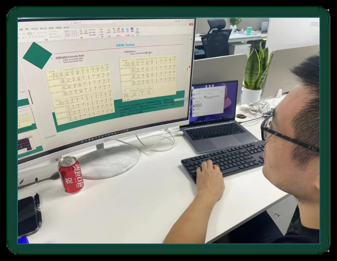
BACKEND TO SIGN-OFF
Physical Design & Layout
Bridge netlist to manufacturable layout with backend planning that stays aligned with foundry rules and sign-off needs.
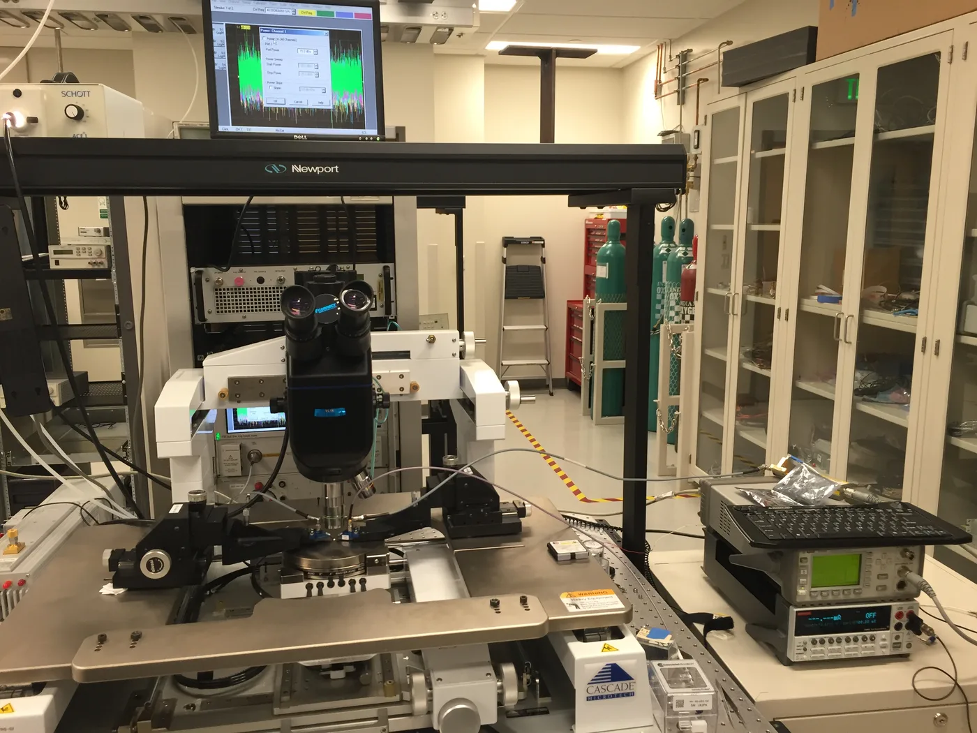
IP FIT BEFORE INTEGRATION PAIN
IP Cores & Licensing
Reduce schedule risk by aligning interface, memory and subsystem IP choices with the actual process and integration path.
Packaging, Test & Delivery
Packaging, test, PCB, firmware, supply chain and turnkey productization.
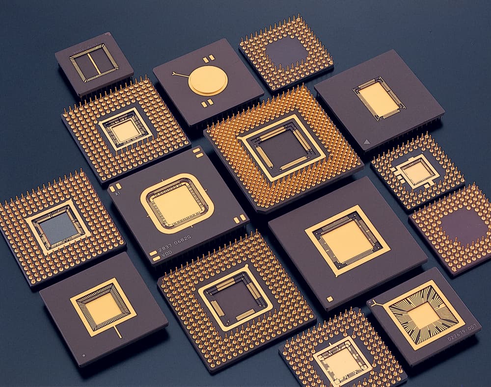
ASSEMBLY PATH TO SHIPPABLE PRODUCT
Semiconductor Packaging
Plan package type, prototype assembly, inspection and qualification early so silicon delivery does not stall after wafer completion.
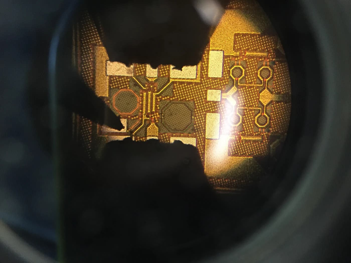
CP · FT · RELIABILITY
Test & Product Engineering
Connect CP, FT and reliability planning so packaged silicon is measurable, debuggable and ready for customer evaluation.
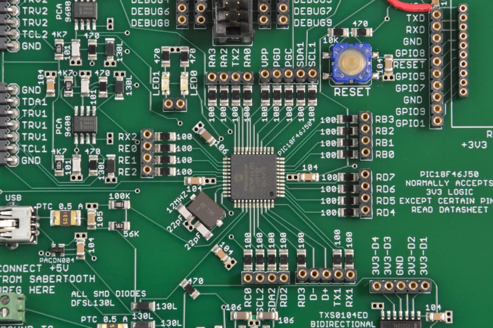
BOARD-LEVEL PRODUCTIZATION
PCB Design & Manufacturing
Support evaluation boards, demo boards and production-minded PCB work that connects packaged silicon to a usable system.
BRING-UP TO DEMO
Embedded Software & Firmware
Connect chip bring-up with firmware, board support and system validation so custom silicon can be demonstrated quickly.
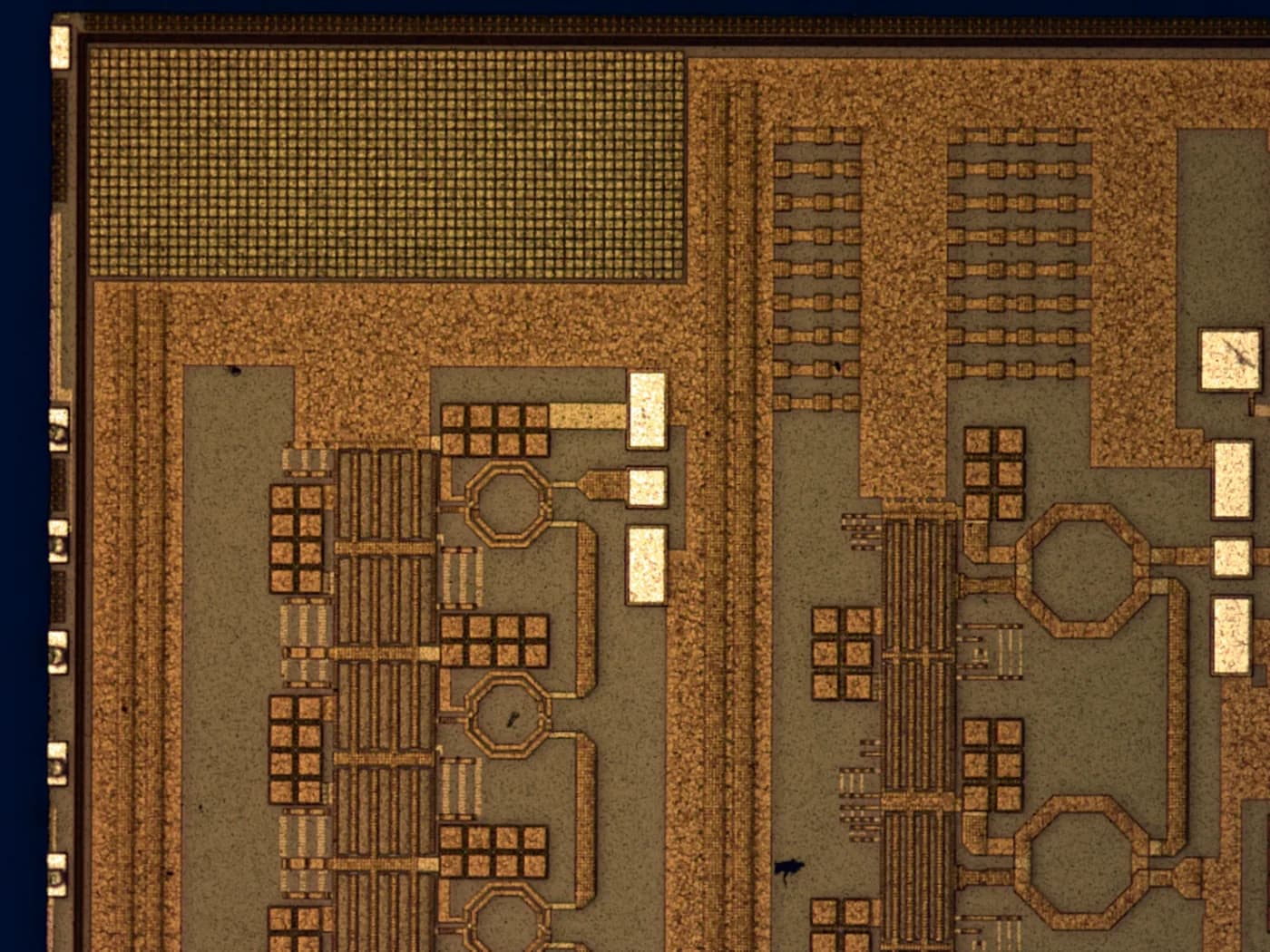
ONE COORDINATED CHAIN
Supply Chain & Logistics
Simplify handoffs across fabs, packaging houses, test providers and international delivery partners.
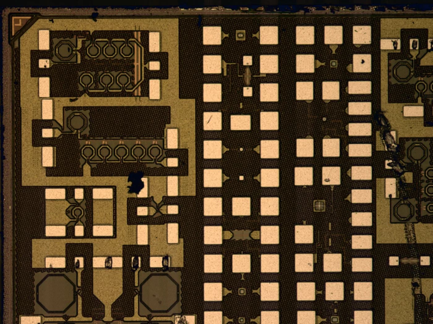
ONE PARTNER · FULL DELIVERY PATH
Turnkey ASIC Solutions
Unify design support, tape-out, packaging, test, board work and delivery under one execution-facing partner.
Execution Flow
One coordinated path from process selection to delivery
Semiconductor programs move through node selection, tape-out, packaging, test and delivery. This page shows how those steps connect, so the path from process choice to delivered samples is clear from the start rather than discovered mid-project.
Scope
Align application, node, volume target, sample goal and delivery constraints before selecting the execution path.
Prepare
Package the design, review manufacturing assumptions and line up the supporting package, test and board plan.
Tape-Out
Coordinate fab submission, shuttle or production milestones and keep communication simple for global stakeholders.
Package & Test
Move wafers into package, CP and FT with the downstream sample or product objective already defined.
Deliver
Ship wafers, packaged parts or evaluation hardware with a cleaner handoff into customer validation or ramp.
Best First Inquiry
Send the project context that affects the service path
- Application or product type
- Preferred process node or process range
- Current project stage, such as architecture, RTL, tape-out ready or sampling
- Expected volume, package preference and target timeline
- Whether you also need package, test, PCB or firmware support