
BOARD-LEVEL PRODUCTIZATION
Board-Level Support for Evaluation and Delivery
Custom silicon only creates business value when it can be demonstrated, validated and integrated into a working system. PCB support bridges that final gap.
QUICK ANSWER
Can TOMPW coordinate chip evaluation boards, demo boards and ATE load boards?
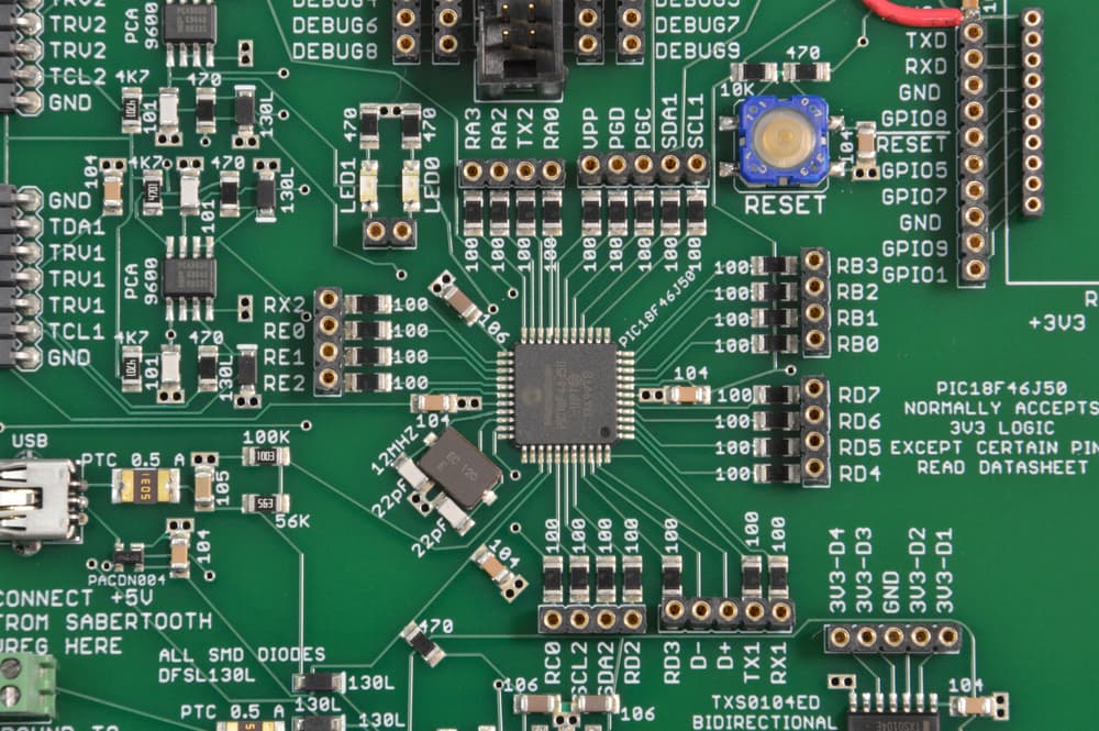
Yes. We coordinate eval / demo boards, reference design kits, HDI ATE load boards, probe card interfaces and bring-up boards for first silicon. Schematic, layout, BOM, fabrication and quick-turn assembly are planned together with the package and test decisions.
Can an eval board be ready before first silicon returns?
Usually yes for the board itself — socketed eval boards are built in parallel with wafer fab so first silicon goes straight into the socket at MPW return. The team can also pre-stage bring-up scripts and instrument configs ahead of silicon arrival.
BOARD FAMILIES
From chip demo to ATE load board — one planning path
Chip programs need several different boards. The categories below cover the typical sequence, from first silicon to production test. Choosing the right type per stage keeps the schedule honest.
| Family | Typical content | Main planning concern |
|---|---|---|
Chip evaluation board Single-device demo / characterization board | Socketed DUT, decoupling, supply tree, comms breakout, status LEDs | Socket type and pin count vs package; supply noise floor for characterization; bring-up sequence (power-on checks → clocks → IO loopback). |
Reference design kit Application-shaped board showing intended use | DUT + companion ICs, example schematic/BOM, gerber package, layout notes | Which parts of the design are intended as customer-modifiable; which are reference-only; lifecycle of the kit vs the silicon. |
Test board (load board / HDI ATE) ATE fixture for production final test | DUT socket, pogo-pin fields, instrumentation paths, controlled-impedance routing | Pin parasitics vs test time budget; handler/prober interface; signal integrity under multi-site parallel test; thermal control under continuous load. |
Probe card / PCB-based probe Wafer-level contact for CP | MEMS probe pins, DUT pad pitch, fanout to tester channels | Pitch vs DUT pad geometry; current carrying per pin; probe cleanliness over many touchdowns; probe-to-tester channel mapping. |
Breakout / daughter board Connector fanout for bench validation | DUT footprint → standard connector (PMOD, Arduino, M.2, etc.) | Which signals are exposed to the user; whether the board needs to be stackable for multi-IC bring-up. |
System-level / bench board SLT or RF bench validation board | DUT + power + IO + instrument access points | Thermal envelope at expected workload; instrument control interfaces (GPIB, USB, LAN); shielding and grounding for RF or high-speed digital. |
Included Scope
What this service is built to handle
- Evaluation and demo board planning around packaged devices
- Board design support connected to package and test assumptions
- Manufacturing coordination for prototype hardware
- Useful for customer samples, demos and firmware bring-up
Best Fit
Common situations where this path makes sense
- ASIC or module teams needing demo hardware
- Programs preparing customer evaluation kits
- Products where board design impacts validation speed
Deliverables
Typical outputs from TOMPW coordination
- Board requirement review
- Prototype PCB coordination
- Demo board planning support
- Alignment with firmware and test activities
CAPABILITY DETAIL
From first bring-up to production test, all on the same planning path
Eval board schematic & BOM planning
Schematic capture with the DUT socketed where practical, power tree sized to the silicon's worst-case envelope, decoupling per the device guide, comms interfaces wired to standard connectors, and a BOM that flags long-lead or single-source parts early.
Layout & signal/power integrity
Stackup choice, controlled-impedance routing for high-speed interfaces, return-path discipline, decoupling placement, ground cuts around RF / high-speed regions, and length matching where protocols require it.
Mechanical & thermal fit
Board outline, mounting holes, connector keep-outs, mechanical interface to the package (exposed-pad solder pad, BGA ball-out, WLCSP under-bump metallization), and thermal relief (thermal vias, copper pours, optional heatsink).
Assembly & quick-turn fabrication
Coordinate prototype fabrication (often 5-15 boards for first silicon), component sourcing, stencil/assembly for fine-pitch parts, and QA. Schedule is fastest when the fab, assembly and component lead times are tracked together.
Load board / HDI ATE design
HDI stackups (any-layer microvia), controlled-impedance routing for tester channels, pogo-pin field placement, DUT socket selection, decoupling local to the DUT, and thermal management for continuous-load production test.
Probe card interface & fanout
Plan the probe card interface for both production wafer sort and engineering probe, including fanout from DUT pad pitch to tester channel pitch, current budget per pin, and probe card maintenance access.
Bring-up & bench validation
Power-on checklist, smoke test plan, clock bring-up, IO loopback, register access via JTAG/SWD/I2C, and a debug path that survives a non-functional silicon return. Coordinated with test planning so coverage matches.
Reference design & customer-facing kit
Take an eval board up to a reference design by adding companion ICs, application schematics, layout notes, BOM with alternates, and a customer-facing documentation set. Useful when the silicon is being released to a customer base.
ENGAGEMENT PATTERNS
Typical shapes of board work
The examples below describe representative forms of engagement. They are illustrative of the type of work and are not specific client records, names, volumes or results.
First-silicon bring-up board
A fabless team needed a bring-up board ready for first MPW silicon return. We coordinated schematic, layout, socket selection, prototype fab and quick-turn assembly so the board arrived in time for first power-on.
ATE load board for mixed-signal device
A mixed-signal ASIC was moving to production test and needed an HDI load board. We coordinated stackup choice, controlled-impedance routing for high-speed channels, pogo-pin field layout, and thermal relief for continuous-load testing.
Customer demo kit for connectivity SoC
A connectivity SoC was being released to a customer base. We extended the eval board into a reference design kit with companion ICs, application schematics, BOM with alternates and a customer-facing documentation set.
RF bench validation board
An RF device needed bench validation beyond FT. We coordinated a bench board with controlled-impedance routing for the antenna interface, shielding, and instrumentation access points so the bench data could be tied back to the FT results.
Execution Notes
Commercially important details buyers usually ask later
- The source package references load board and demo board design directly.
- Board design is closely linked to package selection and test strategy.
- This page improves search relevance for buyers looking beyond wafer-only support.
Next Move
Send package, target stage and end-market together
Board scope changes sharply with end market (consumer vs automotive) and with stage (first silicon vs production test). Sharing package, pinout and target production volume up front keeps the plan honest about lead time and cost.
Email board contextFAQ
Questions buyers ask around eval, demo and test boards
Usually yes for the board itself; socketed designs are built in parallel with wafer fab so first silicon goes directly into the socket at MPW return. The team can also pre-stage bring-up scripts and instrument configs ahead of silicon arrival.
An eval board shows the device working in isolation — DUT socket, power, decoupling, basic comms. A reference design kit adds companion ICs, application schematics, layout notes, BOM with alternates and a customer-facing documentation set so the design can be reproduced or modified by a downstream user.
Load boards are HDI ATE fixtures with controlled-impedance routing, pogo-pin fields, DUT sockets and thermal management for continuous-load test. TOMPW coordinates the design with the ATE platform, handler and test program so the load board is ready when production test starts.
Yes. Probe card interface planning for both engineering probe and production wafer sort is in scope, including pad-pitch fanout, current budget per pin and probe maintenance access. TOMPW is not a probe-card vendor; coordination selects the right partner for the target PDK and pin count.
Indicative lead times are typically a few weeks end-to-end (fab + assembly + component sourcing). The exact schedule is confirmed per project based on stackup, component lead times and assembly complexity. Long-lead or obsolete parts are flagged early to avoid schedule slip.
Common case. The eval board is designed to accept a range of socket adapters so the same board can host MPW samples in one package and full-mask samples in another. We flag this in the schematic/BOM planning stage so the adapter swap is a planned step, not a rework.
Related Services
Adjacent steps in the same silicon program
ASSEMBLY PATH TO SHIPPABLE PRODUCT
Semiconductor Packaging
Plan package type, prototype assembly, inspection and qualification early so silicon delivery does not stall after wafer completion.
CP · FT · RELIABILITY
Test & Product Engineering
Connect CP, FT and reliability planning so packaged silicon is measurable, debuggable and ready for customer evaluation.
BRING-UP TO DEMO
Embedded Software & Firmware
Connect chip bring-up with firmware, board support and system validation so custom silicon can be demonstrated quickly.
ONE PARTNER · FULL DELIVERY PATH
Turnkey ASIC Solutions
Unify design support, tape-out, packaging, test, board work and delivery under one execution-facing partner.
FOUNDRY COVERAGE
Foundries TOMPW coordinates for this path
Board work is foundry-agnostic in principle but the package on the DUT ties back to a specific foundry ecosystem. The foundries below are common partners for programs that go through TOMPW coordination.
PLANNING TOOLS
Calculators that support board-led planning
Estimate unit cost, test cost and tape-out budget while you shape the board plan and the silicon roadmap.
Wafer & Unit Cost Calculator
Turn a wafer run into a per-chip cost: dies per wafer, yield, packaging and test, plus a target margin.
Open tool →Test Cost & Yield Calculator
Estimate ATE test cost per device and per good unit from tester rate, test time, handler cost, volume and test yield.
Open tool →Tape-out Budget Estimator
Full program model: DPW, yield, packaging, HBM, test, NRE and volume → unit cost, price and gross margin.
Open tool →