

Foundry profile
ams OSRAM
ams OSRAM is a leading provider of optical solutions and specialty analog semiconductor processes, running frequent MPW shuttles for analog, mixed-signal and high-voltage designs. TOMPW Service supports ams OSRAM MPW access via authorized channels.
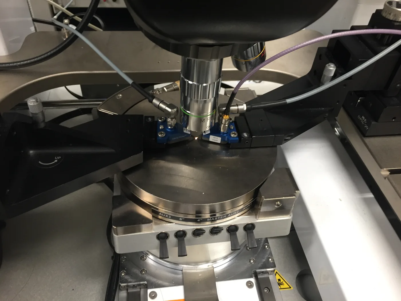
Representative imagery from semiconductor programs we have supported or analysed
Process Nodes
Technologies & Platforms
TOMPW Support Capabilities
Best For
Notes
- ams OSRAM runs one of the most frequent MPW programs in the industry (15+ shuttles annually).
- Access is typically through broker programs such as EUROPRACTICE; TOMPW coordinates the engagement.
Why This Profile Exists
This profile exists so a team can review foundry-specific context directly, while still understanding TOMPW's role in execution, comparison and downstream supply-chain coordination.
Discuss ams OSRAM for Your Program
TOMPW Service can coordinate MPW, NTO and production engagements with ams OSRAM as part of a scoped execution path.
Email for a QuoteCOMMON QUESTIONS
Working with ams OSRAM through TOMPW
Can TOMPW arrange MPW or shuttle runs at ams OSRAM?
Yes. TOMPW coordinates MPW, NTO and full-mask access at ams OSRAM for overseas chip teams, handling scheduling, EDA checks and logistics.
What support does TOMPW provide beyond the wafer at ams OSRAM?
Packaging, final test, PCB support and turnkey assembly coordination through the foundries we coordinate, so the customer sees a simpler handoff path.
How do I get a quote for a ams OSRAM engagement?
Email market@tompwservice.com with your GDSII, target node and volume, or use the quote button. TOMPW returns a scoped execution plan.
RELATED FOUNDRY PROFILES
Other foundries teams compare ams OSRAM with
RELATED SERVICES
Services that pair with a ams OSRAM engagement
MPW / Fab Shuttle
Compare public shuttle windows across foundries, control first-silicon cost and move from tape-out planning to wafer delivery with one execution path.
Learn more →Full Mask / Production Foundry
Move validated designs into dedicated mask production with yield, volume and supply planning support.
Learn more →Semiconductor Packaging
Plan package type, prototype assembly, inspection and qualification early so silicon delivery does not stall after wafer completion.
Learn more →Test & Product Engineering
Connect CP, FT and reliability planning so packaged silicon is measurable, debuggable and ready for customer evaluation.
Learn more →Turnkey ASIC Solutions
Unify design support, tape-out, packaging, test, board work and delivery under one execution-facing partner.
Learn more →MPW / SHUTTLE ACCESS
Plan a ams OSRAM MPW by process node
TOMPW coordinates multi-project wafer runs at ams OSRAM across the nodes below. Open a node to see typical applications, what the run involves and how to book a shuttle slot.