
ASSEMBLY PATH TO SHIPPABLE PRODUCT
Packaging Support That Starts Before Wafers Arrive
Packaging is often where prototype momentum slows down. TOMPW helps customers think through package choice, assembly coordination and the transition into test and delivery.
QUICK ANSWER
What package families can TOMPW coordinate for a chip program?
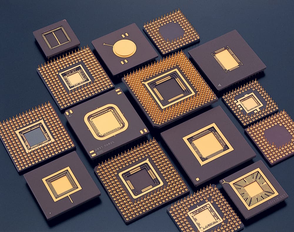
TOMPW helps plan and coordinate QFN/DFN, SOP/SSOP/SOT, BGA/LGA, WLCSP, Flip-Chip and SiP-style modules. The right family depends on IO count, pitch, thermal budget and board constraints — not on a single one-size-fits-all rule.
Can packaging be arranged for MPW wafers?
Yes. Packaging is often the next decision after first silicon, and planning it before wafers are delivered avoids idle time once samples are in hand. We coordinate die singulation, die attach, wire bond, molding and inspection for plastic-mold and laminate-substrate packages.
PACKAGE FAMILIES
Common forms TOMPW helps plan and coordinate
Package choice shapes electrical, thermal and board behavior. The ranges below are typical industry planning ranges, not TOMPW specifications.
| Family | Full name | Typical IO | Typical pitch | Substrate | Typical use |
|---|---|---|---|---|---|
| QFN / DFN | Quad / Dual Flat No-lead | 6 – 100 | 0.4 – 0.65 mm | Copper leadframe with die-pad paddle | Leadless with exposed-pad thermal path; common for analog, RF, mixed-signal and power devices. |
| SOP / SSOP / SOT | Small-outline leaded | 3 – 28 | 0.635 – 1.27 mm | Pre-plated copper leadframe | Leaded, easy board assembly; sensors, low/mid-IO logic, LDO and PMIC devices. |
| BGA / LGA | Ball / Land Grid Array | up to several hundred | 0.4 – 1.0 mm | BT laminate or built-up substrate with solder balls / lands | Area-array for higher IO density and better electrical/thermal behavior; ASIC, SoC, FPGA. |
| WLCSP | Wafer-Level Chip Scale | varies by die | 0.35 – 0.5 mm | Redistribution layer (RDL) on the wafer itself | Die-size package with the shortest interconnect; space/power-constrained mobile and RF devices. |
| Flip-Chip | Flip-Chip bump | high | sub-150 µm bumps | BT / built-up laminate with under-bump metallization | Face-down bumps for best high-frequency and thermal performance; often under a BGA or on board. |
| SiP / Heterogeneous | System-in-Package | module-dependent | — | Mixed: laminate + embedded passives + stacked dice | Multiple dice and passives in one module; RF front-ends, sensor hubs, power modules. |
Included Scope
What this service is built to handle
- Planning across common package families such as QFN/DFN, SOP/SSOP/SOT, BGA/LGA, WLCSP, flip-chip and SiP-type modules
- Quick-turn prototype assembly: die attach, wire bond and plastic mold for engineering lots
- Wafer backgrind and dicing of full-mask and MPW blocks across silicon, glass, sapphire and substrate
- Inspection and failure analysis: 2D/3D X-ray, C-SAM/SAT, decap, cross-section and layer removal
- Reliability and qualification path: HTOL/HAST/burn-in, ESD (HBM/CDM/Latch-up) and AEC-Q100/Q101-style automotive prep
- Coordination with CP, FT, SLT and downstream board-level evaluation
Best Fit
Common situations where this path makes sense
- Teams moving from bare wafer to evaluated product
- Products where package form factor affects electrical or thermal behavior
- Customers that need one coordinator across assembly and test suppliers
Deliverables
Typical outputs from TOMPW coordination
- Package path recommendation inputs
- Assembly coordination
- Package and test handoff alignment
- Sample delivery support
CAPABILITY DETAIL
From package choice to measurable, qualified samples
Package family selection & planning
Early alignment of package choice with die pad layout, thermal budget, board footprint and downstream test or qualification needs. Covers QFN/DFN, SOP/SSOP/SOT, BGA/LGA, WLCSP, Flip-Chip and SiP-type modules.
Quick-turn prototype packaging
Rapid plastic-mold assembly for DFN/QFN and similar leadless forms, plus die attach and wire bonding for engineering lots. Indicative short lead times are available for prototype batches; the exact schedule is confirmed per project and depends on wire type, mold compound and line loading.
Wafer backgrind & dicing
Thinning of 8-inch and 12-inch wafers to thin profiles, and dicing of full-mask and MPW blocks across silicon, glass, sapphire and substrate materials. Street width, tape choice and thin-wafer handling are planned together with the assembly step.
Die attach, wire bond & molding
Substrate and leadframe options, gold and copper wire bonding, and plastic molding for common leadless and leaded forms. Bumping and substrate-based advanced forms are coordinated through the appropriate assembly partner in the network.
Thermal management & heat-path planning
Selection of thermal path (exposed pad, heat spreader, thermal vias, top-side cooling, WLCSP backside), thermal-interface material choices, and customer-board-side copper area / via stack to keep junction temperatures within the operating envelope for the end market.
Signal & power integrity review
Return-path discipline, decoupling placement, impedance-controlled routing for high-speed interfaces, crosstalk mitigation and high-current PDN design. Review happens against the chosen package's breakout density and the customer's board stackup assumptions.
Substrate & leadframe sourcing
Coordinate between laminate (BT / built-up) and leadframe-based packages, including substrate material selection (Tg, CTE), leadframe finish (matte tin, NiPdAu) and pre-plating choices. For advanced packages, ABF / Ajinomoto build-up film and substrate vendor selection are part of the conversation.
Inspection & failure analysis
Non-destructive and physical analysis available as standalone work or as part of debug: 2D/3D X-ray, C-SAM/SAT acoustic imaging, decapsulation, cross-section/polish and layer removal. Useful for incoming inspection, field-return analysis and process learning.
Reliability & qualification path
Preparation for operational-life, moisture and environmental stress flows such as HTOL/HAST/burn-in, ESD characterization (HBM/CDM/Latch-up) and automotive-grade preparation aligned with AEC-Q100/Q101-style requirements. Plans are scoped per device and end market.
Test coordination
Wafer sort (CP), final test (FT) and system-level test (SLT) planning, load-board and handler alignment, and ATE platform coordination so packaged silicon is measurable and debuggable before customer evaluation.
THERMAL MANAGEMENT
Heat-path planning across package families
Thermal behavior is part of package selection, not an afterthought. The table below maps common heat-path approaches to package type and the kind of device they typically support. The exact resistance numbers depend on the package, the customer's board copper layout and the airflow in the end product.
| Thermal path | Best for | Typical resistance band |
|---|---|---|
| Exposed die-pad (QFN/DFN) | Power management, RF PA, motor driver, LED driver | θJA in the tens of °C/W range, depending on PCB copper area |
| Heat-spreader BGA / lid | High-power ASIC/SoC, FPGA, multi-die modules | θJA typically in the single-digit °C/W range under forced-air cooling — actual value depends on package size, PCB copper area, TIM and airflow |
| Thermal vias under exposed pad | All QFN/DFN-style leadless packages on customer PCB | Improves θJA by 30-60% vs no-via board, depending on via count and copper |
| Top-side cooling / heatsink attach | High-TDP SoC, automotive ECU, server-class silicon | Driven by TIM (thermal interface material) choice and heatsink design |
| WLCSP backside cooling | Mobile PMIC, RF front-end, small die with tight thermal envelope | Driven primarily by PCB copper area and via count |
SIGNAL & POWER INTEGRITY
SI / PI knobs that matter at the package boundary
For BGA, flip-chip and high-speed packages, signal and power integrity decisions at the package boundary often determine whether the design works on the customer board. The topics below are the recurring ones for package-level SI/PI review.
Return-path discipline in BGA fanout
For BGA and flip-chip packages, ground/power return paths under the die need continuous reference planes. Breaks in the return path cause resonant impedance spikes that show up as SI/PI issues at high speed.
Power-delivery network (PDN) decoupling
Bulk, mid-frequency and high-frequency decoupling are placed as close to the die pads as possible, with package-level and on-die capacitance layered. For high-current transients, VRM loop bandwidth and bulk capacitor ESR matter as much as the on-board layout.
Impedance-controlled routing
DDR, PCIe, USB, MIPI, Ethernet and SerDes all require controlled single-ended or differential impedance. Stackup choice (core/prepreg thickness, copper weight) sets the achievable impedance; the layout follows the stackup target with verified tolerance.
Crosstalk mitigation
Aggressor/victim spacing, guard traces/vias, and differential pair symmetry all reduce crosstalk. For dense BGA breakouts, the choice between dog-bone fanout and via-in-pad can change achievable breakout density by up to roughly 2-3x depending on ball pitch and layer count.
High-current / low-impedance power planes
Power-hungry SoCs need wide copper pours or multiple planes stitched with sufficient vias. For packages with exposed-pad current paths, via placement under the pad needs to balance current-carrying capacity vs thermal relief for solder joint reliability.
ENGAGEMENT PATTERNS
Typical shapes of packaging work
The examples below describe representative forms of engagement. They are illustrative of the type of work and are not specific client records, names, volumes or results.
RF / mixed-signal QFN quick-turn prototype
An early-stage fabless team needed first packaged samples of an RF transceiver in a leadless QFN to begin board evaluation. TOMPW coordinated die singulation, gold wire bond and plastic mold on a short prototype lead time, then handed off to final test.
BGA field-return failure analysis
A shipped module exhibited intermittent behavior. Non-destructive 2D/3D X-ray and C-SAM located a suspected anomaly, followed by decap and cross-section to confirm the failure mechanism — feeding a corrective-action loop without disclosing the end customer.
Power IC DFN wire-bond prototype
A power-management device targeted a thermally enhanced DFN. TOMPW arranged thin-wafer handling, copper wire bond and exposed-pad molding so the team could validate thermal and electrical behavior on real samples.
Automotive-sensor reliability prep
A sensor entering a vehicle platform needed automotive-grade reliability evidence. TOMPW helped structure HTOL/HAST and ESD characterization aligned with AEC-Q100/Q101-style flows and a defined sample plan.
BGA fanout SI/PI review before customer release
A team was about to release a BGA-packaged SoC to a customer base. We reviewed the customer-board breakout, return-path continuity and PDN layout against the package's breakout density, and flagged the two corners where impedance and decoupling margin were tight.
Package change during MPW-to-mask transition
An RF device moved from a QFN prototype package to a smaller WLCSP for full mask. We coordinated the die-pad remap, the redistribution layer design and the new package qualification path so the schedule held for the second tape-out.
SiP module for a sensor hub
A sensor hub needed to combine an ASIC die, an MCU die and several passives in one module. We coordinated the substrate design, stacked-die assembly and overmold so the SiP came back as a single drop-in part.
Execution Notes
Commercially important details buyers usually ask later (kept)
- Package choice should be aligned with test, board and end-market qualification needs from the start.
- Lead times for prototype assembly are indicative and confirmed per project based on wire type, mold compound and line loading.
- Inspection and failure analysis can be arranged as standalone work or as part of a broader debug engagement.
- Package choice is often driven by board, thermal and qualification constraints rather than by the foundry alone, so it should be settled alongside node selection.
Next Move
Share node, schedule and downstream requirements together
The right recommendation depends on more than one keyword. Package, CP, FT and sample goals often change whether MPW, NTO or a broader turnkey path makes the most sense.
Email project contextFAQ
Questions buyers ask around packaging
Yes. Packaging is often the next decision after first silicon, and planning it before wafers are delivered avoids idle time and rework once samples are in hand.
Common leadless (QFN/DFN), leaded (SOP/SSOP/SOT), area-array (BGA/LGA), wafer-level (WLCSP), flip-chip and SiP-type modules. The right choice depends on IO count, pitch, thermal budget and board constraints.
Short indicative lead times are available for prototype batches of plastic-mold leadless and leaded forms with die attach and wire bonding. The exact schedule is confirmed per project based on wire type, mold compound and line loading.
Yes. 2D/3D X-ray, C-SAM/SAT, decapsulation, cross-section and layer removal can be arranged on their own or as part of a broader debug engagement.
TOMPW can help structure HTOL/HAST/burn-in, ESD (HBM/CDM/Latch-up) and AEC-Q100/Q101-style automotive preparation with a defined sample and test plan.
Package choice, sample readiness and qualification flow are downstream decisions that shape cost and schedule. Planning them early avoids idle time after wafers return and prevents rework once the first samples are already in hand.
Common paths include exposed die-pad with thermal vias, heat-spreader BGA with lid attach, top-side heatsink with TIM, and WLCSP backside cooling. The right path depends on package type, TDP envelope and customer-board copper area.
Return-path discipline under the die, controlled-impedance routing out of the BGA breakout, and PDN decoupling close to the die are the core knobs. For dense breakouts, via-in-pad can increase achievable breakout density by 2-3x versus dog-bone fanout.
Standard BT laminate is sufficient for most BGA up to mid-density. Built-up (ABF/Ajinomoto build-up film) substrates are needed for fine-pitch flip-chip and high-I/O ASIC/SoC packages, and for high-speed signal routing. Substrate vendor selection is part of the package sourcing conversation.
Related Services
Adjacent steps in the same silicon program
LOWER NRE · FASTER FIRST SILICON
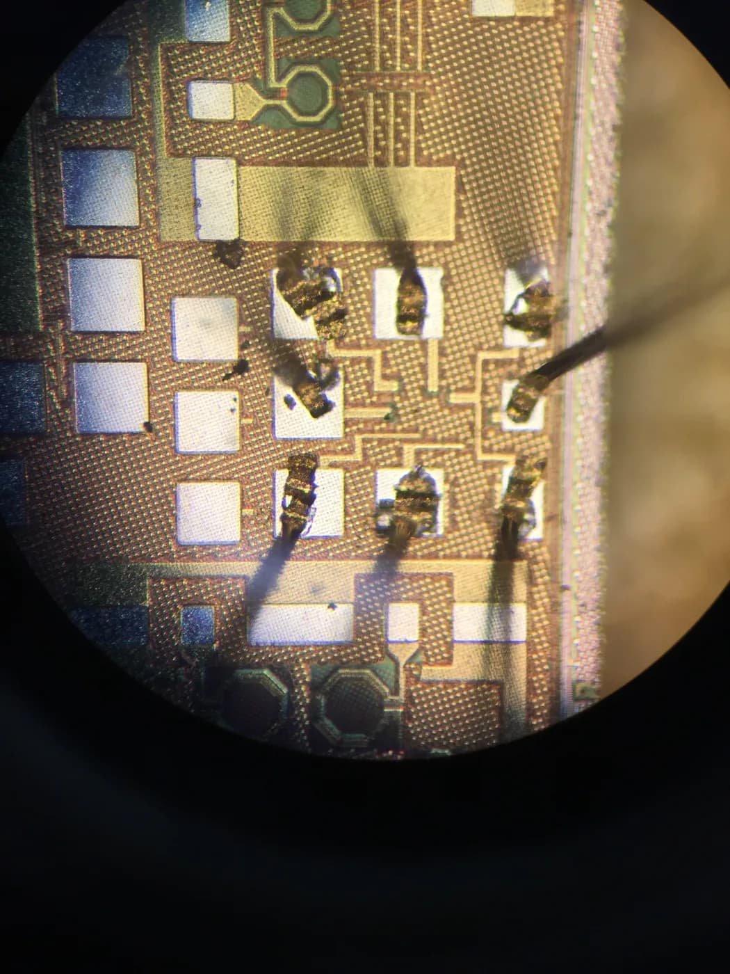
MPW / Fab Shuttle
Compare public shuttle windows across foundries, control first-silicon cost and move from tape-out planning to wafer delivery with one execution path.
CP · FT · RELIABILITY
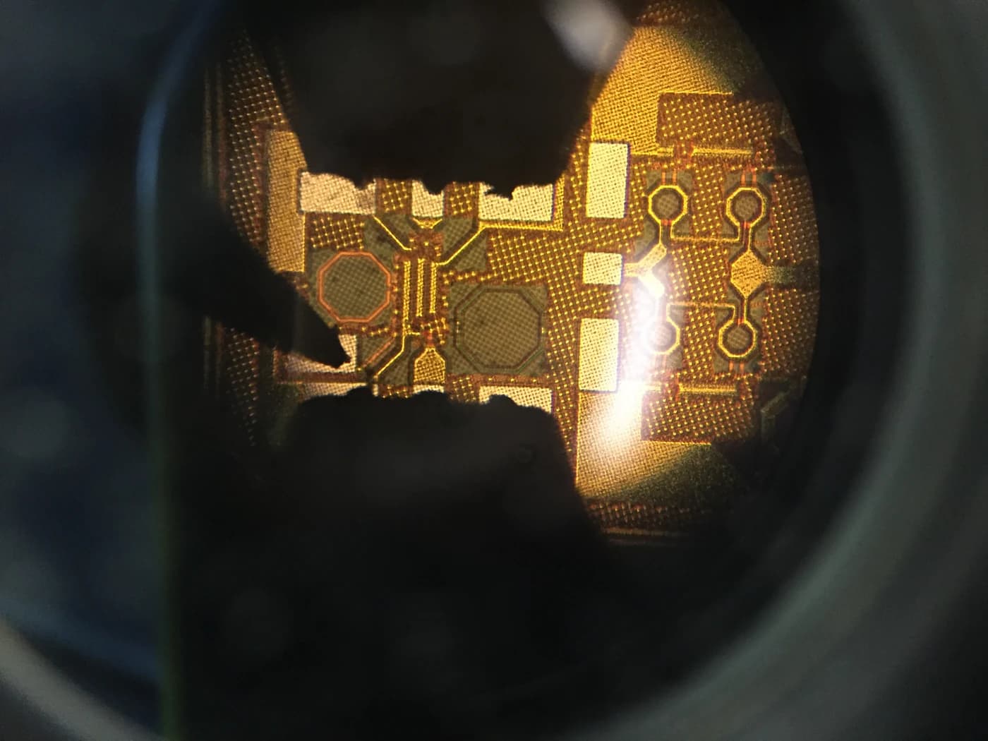
Test & Product Engineering
Connect CP, FT and reliability planning so packaged silicon is measurable, debuggable and ready for customer evaluation.
BOARD-LEVEL PRODUCTIZATION
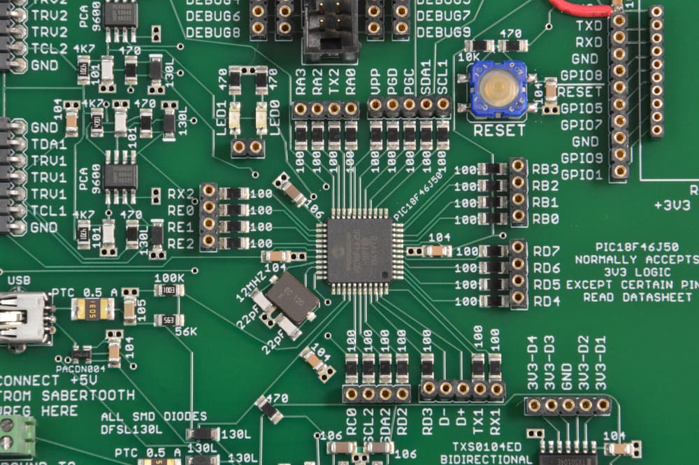
PCB Design & Manufacturing
Support evaluation boards, demo boards and production-minded PCB work that connects packaged silicon to a usable system.
ONE PARTNER · FULL DELIVERY PATH
Turnkey ASIC Solutions
Unify design support, tape-out, packaging, test, board work and delivery under one execution-facing partner.
FOUNDRY COVERAGE
Foundries TOMPW coordinates for this path
Packaging engagements are planned across TOMPW's foundry network, from advanced logic to mature analog, compound and specialty processes.
PLANNING TOOLS
Calculators that support Semiconductor Packaging
Estimate dies per wafer, split shared-mask cost and model unit economics for this path.