
CP · FT · RELIABILITY
Test Planning That Protects the Value of Each Tape-Out
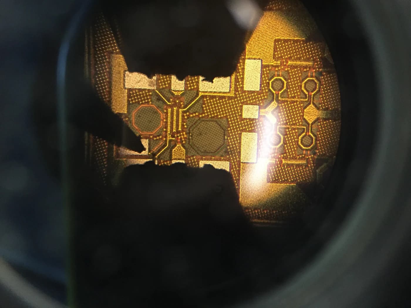
Good silicon still needs a workable test path. TOMPW helps customers think through wafer sort, final test, load board needs and reliability preparation as part of the total delivery chain.
QUICK ANSWER
Does TOMPW coordinate wafer sort (CP), final test (FT) and reliability prep?
Yes. Test planning is part of the delivery chain, not a late-stage separate task. We coordinate CP, FT, system-level test, reliability prep (HTOL / HAST / ESD), yield analysis and failure-analysis handoff so packaged silicon is measurable and debuggable before customer evaluation.
Which test platforms can TOMPW work with?
TOMPW is not an ATE vendor. We coordinate with V93000-class, Teradyne, Chroma and similar mixed-signal / RF platforms, plus bench setups for RF and high-speed validation. The right platform is selected per project, not from a fixed list.
TEST FLOW
Wafer sort to customer samples, all coordinated
A coherent test path runs from wafer probe through reliability prep. The list below is the typical sequence; each step can be scoped as standalone work or as part of a broader delivery plan.
- STEP 01
Test strategy & program planning
CP/FT split, binning, DPPM target
- STEP 02
CP — wafer sort
Probe card, prober interface, alignment
- STEP 03
FT — final test
Load board, ATE platform, test time
- STEP 04
Test program bring-up
Pattern translation, shmoo, characterization
- STEP 05
Reliability prep
HTOL, HAST, ESD, burn-in planning
- STEP 06
Yield analysis & DPPM tracking
Per-lot trends, outlier lot review
- STEP 07
System-level & board-level test
SLT, bench validation
- STEP 08
Failure analysis handoff
X-ray, C-SAM, decap, cross-section, FA
Included Scope
What this service is built to handle
- Coordination for wafer sort and final test planning
- Load board and demo-board related preparation inputs
- Reliability and environmental test support path
- Alignment with package, board and customer-evaluation milestones
Best Fit
Common situations where this path makes sense
- Programs preparing engineering samples for end-customer review
- Products needing CP/FT planning before assembly starts
- Teams that do not want test to become a last-minute bottleneck
Deliverables
Typical outputs from TOMPW coordination
- Test path review
- CP and FT coordination inputs
- Reliability planning support
- Board-level evaluation alignment
CAPABILITY DETAIL
From CP planning to DPPM-tracked, qualified parts
Test strategy & program planning
Early definition of the test path: which device parameters must be screened at CP vs FT, how production-level binning affects probe time and yield, and what failure-mode coverage the test program needs to deliver before customer samples ship.
Wafer sort (CP) coordination
Probe card design inputs, prober/handler interface, alignment to die-level pad layout and street plan. Coordinates with wafer backgrind/dicing and probe-card supply timing so CP doesn't sit idle waiting on hardware.
Final test (FT) & ATE coordination
Load board and socket planning, ATE platform selection (V93000, Teradyne, STS, etc. — chosen per project), test-time budget, and binning definition aligned with the product spec. Coordinated with package-level test access.
Test program development & bring-up
Pattern translation from simulation vectors, shmoo and characterization support, datalog-driven debug and DPPM target setting. Bring-up is most efficient when the package, pin map and ATE platform are already locked.
Reliability & qualification prep
HTOL, HAST, temperature cycling, ESD (HBM/CDM/Latch-up) and burn-in planning, sample allocation and read-point scheduling. Aligned with end-market requirements (consumer, industrial, automotive per AEC-Q100/Q101-style flows).
System-level & board-level test alignment
For products that ship as a module or board, plan SLT and bench-level validation alongside the FT program so coverage extends beyond the silicon die. Useful for RF and mixed-signal devices where final behavior emerges at the board level.
Yield analysis & DPPM tracking
Per-lot yield review, parametric tracking, outlier lot analysis and continuous DPPM trending. Feedback loop into test program tuning and into upstream wafer-process improvement conversations with the foundry.
Failure analysis handoff
When a part fails CP/FT or returns from the field, hand off cleanly to FA: 2D/3D X-ray, C-SAM, decap, cross-section, nanoprobing, FIB or TEM as needed. Coordinated with the packaging FA path so the same package isn't analyzed twice.
ENGAGEMENT PATTERNS
Typical shapes of test and product engineering work
The examples below describe representative forms of engagement. They are illustrative of the type of work and are not specific client records, names, volumes or results.
MPW-to-NTO test program port
A fabless team had validated a design on MPW but needed a production-ready test program before NTO. We coordinated pattern translation, characterization shmoos, and probe-card rev to keep the schedule on track.
Multi-site test time reduction
A mixed-signal ASIC was burning test budget on a single-site FT. We helped redesign the test plan for multi-site parallelism, cut ATE time per unit, and coordinated the load-board change without disrupting the existing supply.
Automotive-grade reliability alignment
A sensor entering a vehicle platform needed automotive-grade qualification evidence. We helped structure HTOL/HAST and ESD characterization aligned with AEC-Q100/Q101-style flows and a defined sample plan.
RF bench validation alongside FT
An RF device needed bench-level validation in addition to FT. We coordinated the bench setup (instrumentation, fixtures, automation) so bench-level yields and FT yields could be compared lot-by-lot.
Execution Notes
Commercially important details buyers usually ask later
- Source material explicitly lists CP, FT, load board, demo board, reliability and environmental test support.
- Test planning is most effective when defined before package lock, not after.
- This site positions TOMPW as a program coordinator, not as a standalone tester brand.
Next Move
Send device, package and end-market context together
Test scope changes sharply with end market (consumer vs automotive) and with package (QFN vs BGA). Sharing that context up front keeps the test plan honest about lead time and cost.
Email test contextFAQ
Questions buyers ask around test and product engineering
Sample delivery slips, debug slows and customer evaluation is delayed. Load-board and probe-card lead times are often longer than the wafer fab cycle, so test belongs in the commercial conversation early — not hidden until after contract signing, when options are already limited.
No. The coordination can include wafer sort (CP), final test (FT), system-level test (SLT), reliability and qualification prep, yield analysis and FA handoff. TOMPW treats test as part of the delivery chain, not a separate late-stage task.
Yes. Test access, package pin-out and load-board layout all interact. Coordinating CP/FT planning with package planning avoids pad-access issues and re-spins of either the test hardware or the package.
TOMPW is not an ATE vendor. Coordination commonly covers V93000-class, Teradyne, Chroma and similar mixed-signal/RF platforms, plus bench-level setups for RF and high-speed validation. The right platform is selected per project, not from a fixed list.
Yes. Consumer and industrial reliability plans use a lighter version of the same HTOL/HAST/ESD frameworks, with sample size and read-points scaled to the application. AEC-Q100/Q101-style automotive prep is added only when the device is targeting vehicle platforms.
Per-lot yield review with parametric tracking and outlier lot analysis, plus a continuous feedback loop into test program tuning and into upstream wafer-process conversations with the foundry. DPPM targets are set against the end-product spec, not generic benchmarks.
Related Services
Adjacent steps in the same silicon program
ASSEMBLY PATH TO SHIPPABLE PRODUCT
Semiconductor Packaging
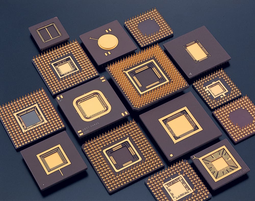
Plan package type, prototype assembly, inspection and qualification early so silicon delivery does not stall after wafer completion.
BOARD-LEVEL PRODUCTIZATION
PCB Design & Manufacturing
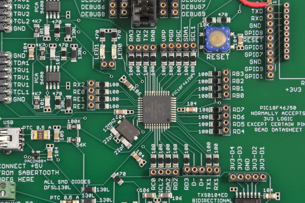
Support evaluation boards, demo boards and production-minded PCB work that connects packaged silicon to a usable system.
ONE COORDINATED CHAIN
Supply Chain & Logistics
Simplify handoffs across fabs, packaging houses, test providers and international delivery partners.
ONE PARTNER · FULL DELIVERY PATH
Turnkey ASIC Solutions
Unify design support, tape-out, packaging, test, board work and delivery under one execution-facing partner.
FOUNDRY COVERAGE
Foundries TOMPW coordinates for this path
Test planning is foundry-agnostic in principle but tightly tied to wafer probe and reliability infrastructure in practice. The foundries below are common partners for programs that go through TOMPW coordination.
PLANNING TOOLS
Calculators that support test planning
Estimate test cost per unit and per wafer, with yield scenarios for different volume bands.