TOMPW Service logo
TOMPW

LOWER NRE · FASTER FIRST SILICON

MPW Shuttle Access for Early Silicon Programs

Use multi-project wafer runs to validate designs without committing to a dedicated mask set. TOMPW helps teams compare node fit, public shuttle timing, tape-out readiness and downstream package or test implications before locking a slot.

Prototype ASIC or SoC validationSensor, analog and mixed-signal proof-of-concept siliconTeams testing market demand or customer sampling before full production commitment
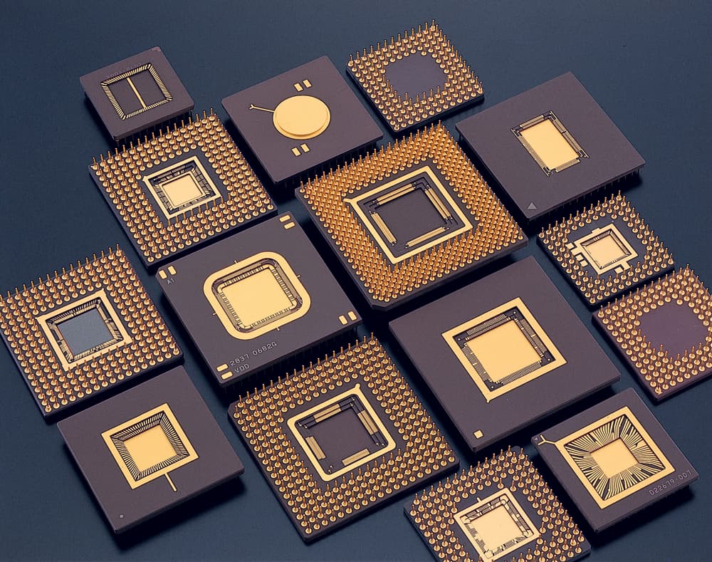
Semiconductor wafer used to illustrate MPW shuttle service

PROCESS SELECTION

Process areas to discuss

Start with the device and system requirements. TOMPW can scope a process review and the downstream package and test work needed to turn a wafer run into usable samples.

The references below describe public technology capabilities. Process selection, PDK access, prototype quantities, packaging and delivery dates are confirmed for each project after technical and commercial review.

CMOS, BCD, high voltage and SOI

Compare digital and mixed-signal CMOS, BCD, HV CMOS and SOI routes for controllers, sensing, interfaces and power-management ICs.

Bring to the review
Function, node or PPA target, voltage domains, isolation, memory options and expected volume.
Review deliverables
A process shortlist, required PDK and IP checks, and a tape-out preparation plan.
Confirm before selection
Device modules, metal stack, IP rights and prototype options vary by platform and run.

Official capability references
RF, mmWave and compound semiconductors

Evaluate SiGe BiCMOS, RF-SOI, GaAs and GaN-on-SiC against noise, power, frequency and integration requirements.

Bring to the review
Frequency band, gain and noise targets, output power, bias conditions, die limits and package interfaces.
Review deliverables
A platform comparison with RF package, probe and characterization requirements.
Confirm before selection
RF GaN and switching-power GaN need separate device and qualification reviews.

Official capability references

SiC devices and GaN power ICs

Review SiC MOSFET and diode manufacturing paths, GaN devices and GaN-on-SOI options for monolithic power circuits.

Bring to the review
Bus voltage, current, switching topology and frequency, thermal limits, device type and package target.
Review deliverables
A device and process feasibility review, plus prototype, assembly and electrical test requirements.
Confirm before selection
Standard MPW, dedicated runs and customer-specific development are different routes; device access and acceptance must be confirmed.

Official capability references

High-temperature SiC circuits

Explore 4H-SiC CMOS for sensing and control where the operating environment exceeds the practical range of conventional silicon circuits.

Bring to the review
Operating temperature, lifetime, voltage, sensor interface and required characterization conditions.
Review deliverables
An initial feasibility review and a characterization plan for the proposed environment.
Confirm before selection
This is an early-access research direction, separate from vertical SiC power-device production. Availability and maturity require a project review.

Official capability references

MEMS and PiezoMEMS

Review silicon, SOI and piezoelectric microsystem routes for sensors, resonators and actuators, together with their packaging needs.

Bring to the review
Mechanical stack, materials, geometry, sensitivity or displacement, release steps and environmental requirements.
Review deliverables
A process compatibility review and a wafer-level, package and functional test plan.
Confirm before selection
Custom process development, release and cavity or hermetic packaging can determine cost and schedule; some piezoelectric routes remain at prototype maturity.

Official capability references

Silicon, SiN and InP photonics

Compare silicon and silicon-nitride passive circuits, active InP platforms and III-V integration for optical routing, modulation, detection and light generation.

Bring to the review
Wavelength, optical budget, active functions, coupling method, electrical interfaces and packaging constraints.
Review deliverables
A platform shortlist and an optical coupling, packaging and characterization plan.
Confirm before selection
Standalone InP fabrication and III-V integration on silicon are different routes. Confirm PDK functions, post-processing, sample format and optical test scope.

Official capability references

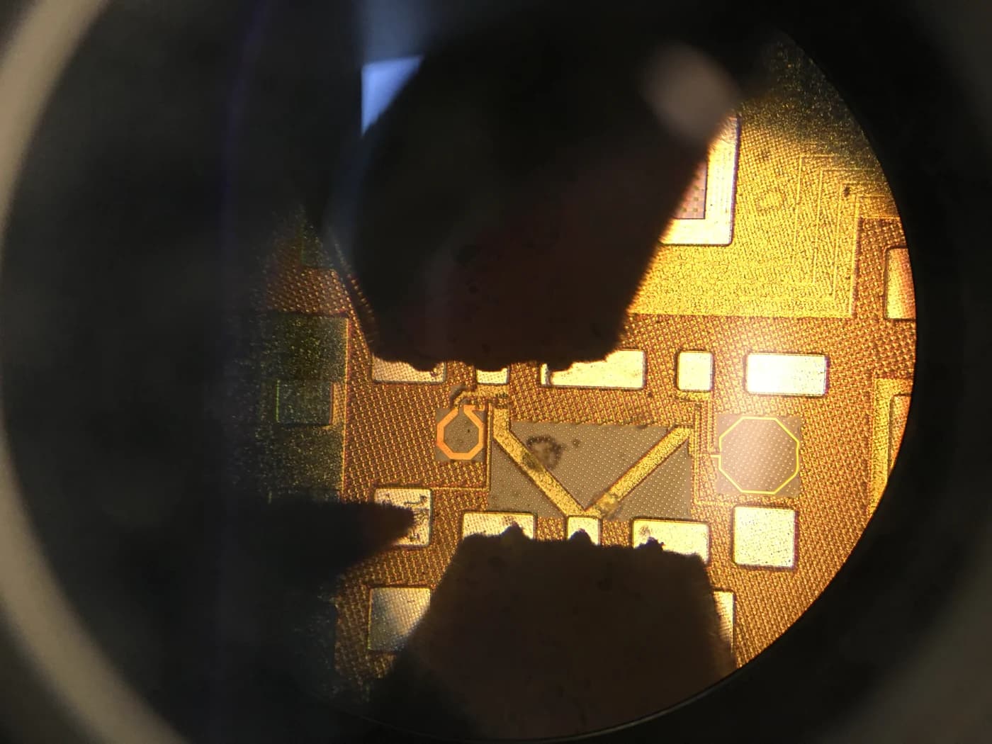
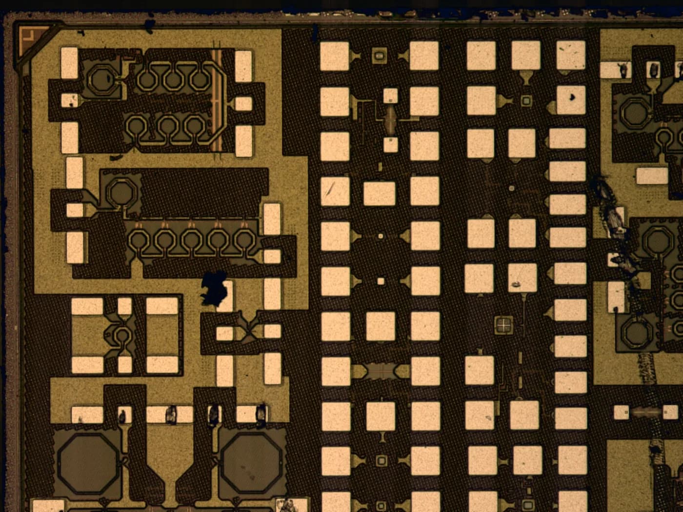
Die probe on a TOMPW-coordinated LNA tape-out
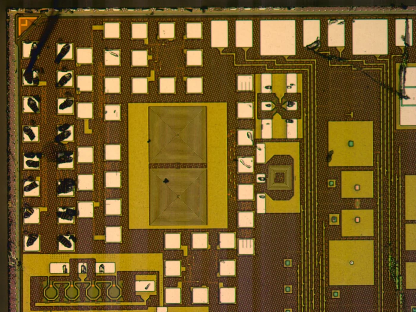
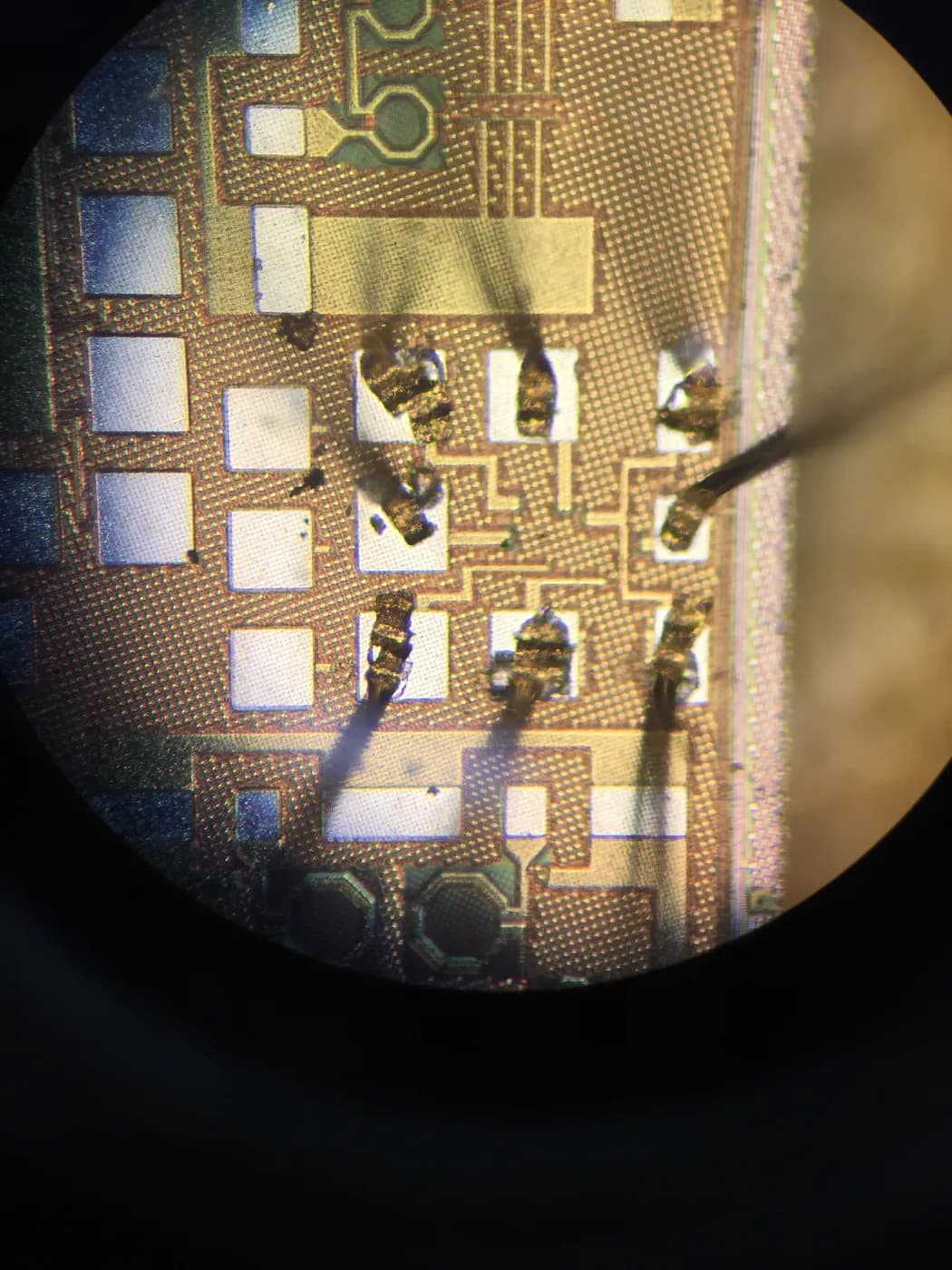
Switch die probed during a TOMPW tape-out
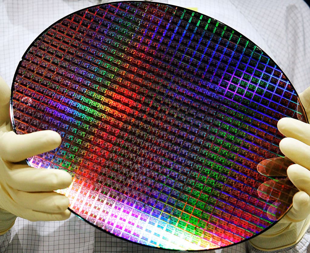
Wafer from a TOMPW-coordinated MPW run
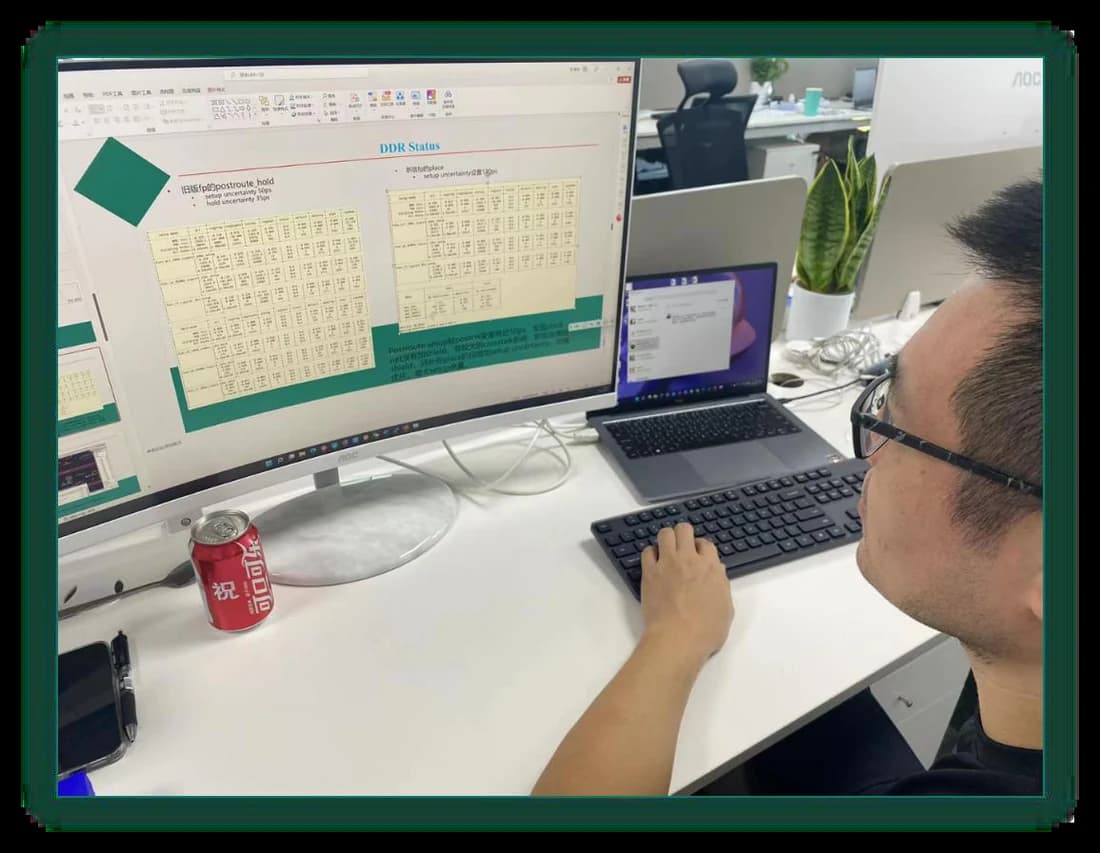
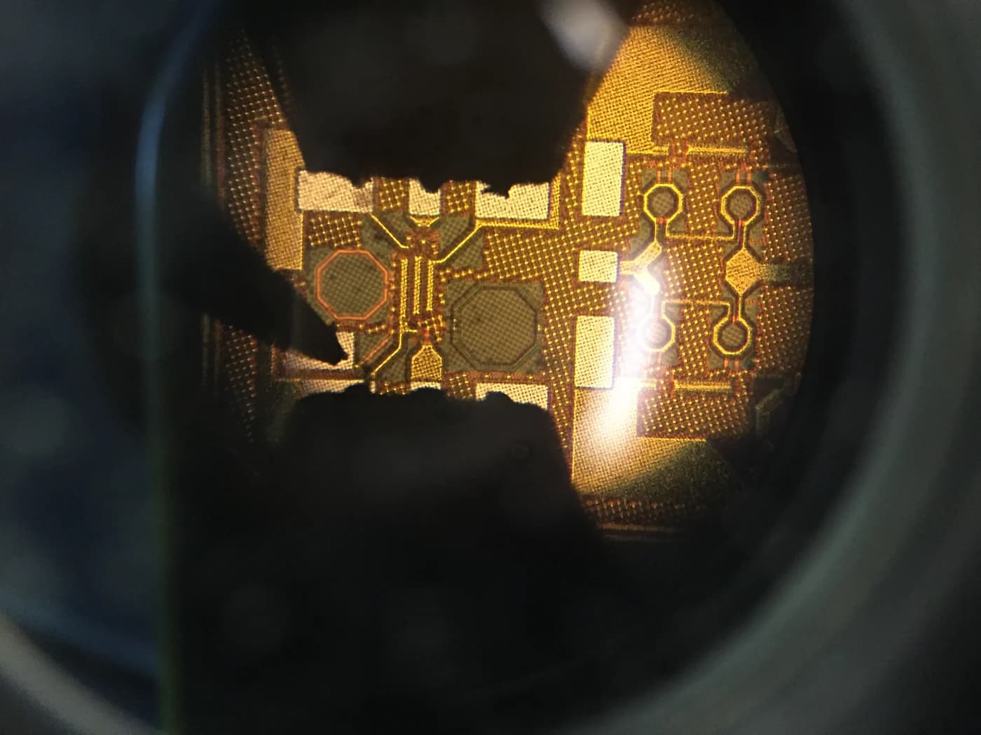
EDA close-up from a TOMPW-tracked design review

Included Scope

What this service is built to handle

  • Shared-mask shuttle entry for prototype and low-volume programs
  • Multi-foundry window visibility across TSMC, UMC, SMIC, GlobalFoundries and selected specialty platforms
  • Tape-out package review, foundry communication and milestone tracking
  • Commercial and operations coordination from slot selection into wafer delivery

Best Fit

Common situations where this path makes sense

  • Prototype ASIC or SoC validation
  • Sensor, analog and mixed-signal proof-of-concept silicon
  • Teams testing market demand or customer sampling before full production commitment

Deliverables

Typical outputs from TOMPW coordination

  • Shuttle window and node alignment
  • Tape-out checklist review
  • Foundry submission coordination
  • Wafer delivery timeline and status communication

Execution Notes

Commercially important details buyers usually ask later

  • Standard coverage in source material spans 12nm to 3um, with below-7nm handled case by case.
  • Common platforms include CMOS, BCD, SOI and selected specialty processes.
  • Public shuttle calendars usually cluster around recurring month windows rather than one-off opportunities. Typical reference months include spring and autumn slots for advanced-node MPW, plus broader January to December coverage on selected 16nm, 28nm and mature mixed-signal platforms.
  • Public programs from TSMC, UMC and GlobalFoundries also show that availability differs by node, operator and submission rule. Some platforms run only twice a year, while others offer multiple windows across the year.
  • Published shuttle dates are normally GDS submission deadlines rather than wafer-out dates. Registration, export-control review, PO timing and package or test scope need to be aligned earlier, so final slot confirmation should be handled by email or direct project discussion.

Next Move

Share node, schedule and downstream requirements together

The right recommendation depends on more than one keyword. For example, package, CP, FT and sample goals often change whether MPW, NTO or a broader turnkey path makes the most sense.

Email project context

HOW MPW SCHEDULING WORKS

From shared mask to a confirmed shuttle slot

A multi-project wafer run places several customer designs on one mask set, so each team pays only for its portion of the wafer. Most teams use MPW for first silicon, architecture validation, early customer sampling or low-volume research — anywhere the goal is learning rather than immediate high-volume production.

Shuttles follow a monthly or quarterly cadence that depends on foundry, node, process maturity and demand. Missing a tape-out deadline usually means waiting for the next window, so slot selection and downstream package or test planning should start early.

FAQ

Questions buyers ask around MPW / Fab Shuttle

Choose MPW when your priority is low-cost first silicon and design learning rather than volume efficiency. It is the standard entry point for prototypes, design validation and early customer sampling before committing to a dedicated full-mask production run.

No. TOMPW can also review your tape-out package, coordinate foundry communication and extend the flow into packaging, test and logistics when needed. Most customers use it as an execution partner, not only a wafer-order channel.

Related Services

Adjacent steps in the same silicon program

FOUNDRY COVERAGE

Foundry profiles to compare for this path

Compare public technology profiles for MPW / Fab Shuttle, from advanced logic to mature analog, compound and specialty processes. PDK access, contracting route and current availability are confirmed for each project.

PLANNING TOOLS

Handoff checks and planning tools

Review declared handoff inputs with local-only checks, and keep cost and die-count estimates separate from engineering approval.