TOMPW Service logo
TOMPW

Case Studies

From chip samples to evaluation

A closer look at project work supported by TOMPW: RF die inspection, carrier-board assembly, packaged samples and board-level evaluation. Original project photographs show the hardware at each stage.

Selected Project Work

Real hardware, with a clear project scope

Each example pairs a physical sample with TOMPW's role and the stage it supports. The RF die close-up and wire-bonded assembly offer complementary views of sample and assembly work. Customer identities and detailed design data remain confidential.

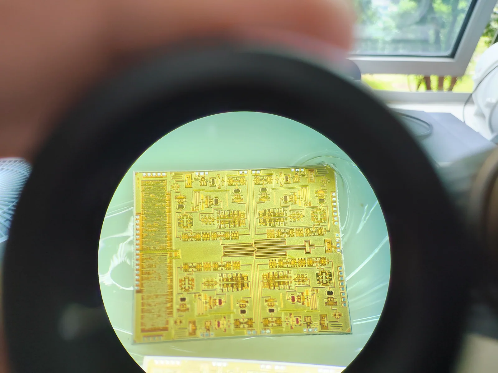
Microscope close-up of an RF die showing circuit features, peripheral pads and fine bond wires.
Microscope view of the RF die and its peripheral connections.

Sample Inspection

RF Die Close-Up

A microscope view shows the RF die’s circuit features, peripheral pads and connections, providing a visual reference for sample inspection, assembly discussions and evaluation planning.

TOMPW scope
TOMPW supported sample inspection, assembly coordination and RF evaluation planning.
Project stage supported
A physical sample and microscope reference for reviewing die connections and preparing the next evaluation step.
Test & product engineering
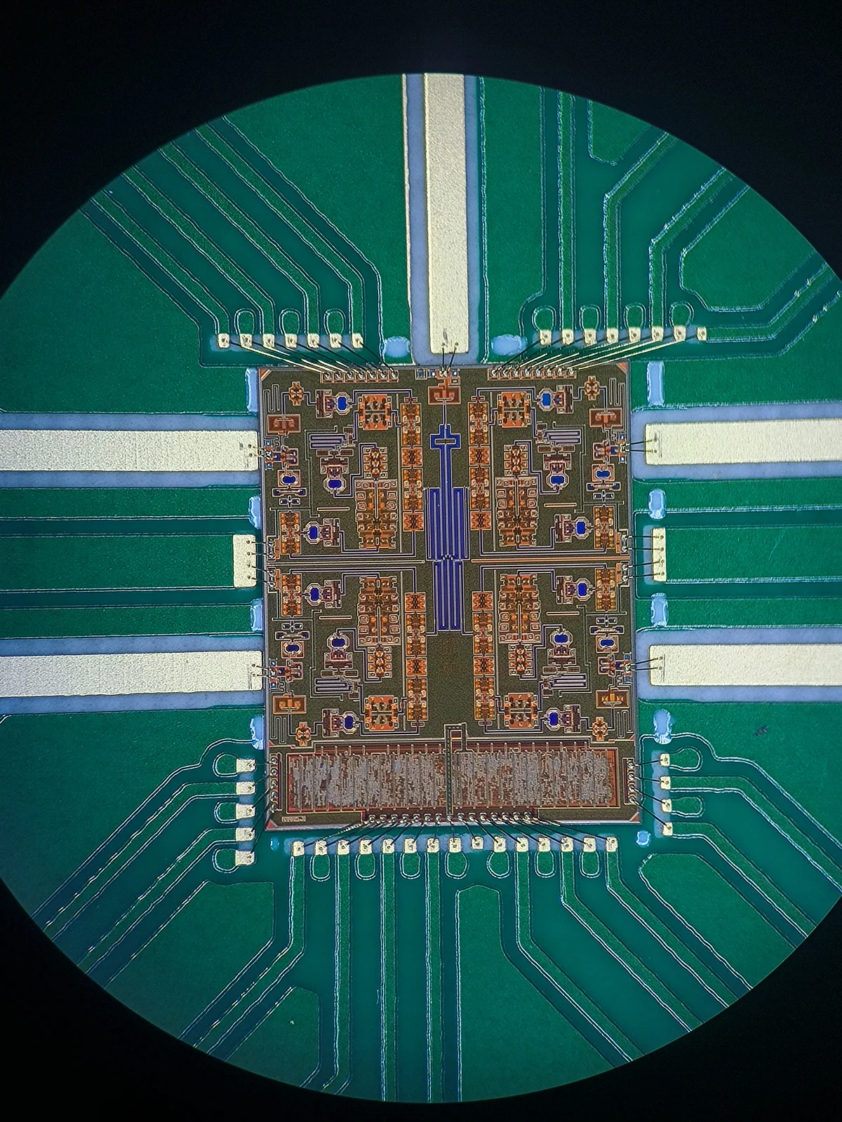
Bare die mounted on a green carrier board with wire bonds connecting its pads to board traces.
Die-to-board wire bonds provide external connections for evaluation.

Assembly & Interconnect

Die Assembly & Wire Bonding

Carrier-board assembly and wire bonding connect die pads to external test interfaces, preparing samples for power-up, functional evaluation and RF measurements.

TOMPW scope
TOMPW coordinated carrier-board assembly, wire bonding and the sample handoff for evaluation.
Project stage supported
A wire-bonded carrier-board assembly with accessible die connections for the next test stage.
Packaging & assembly support
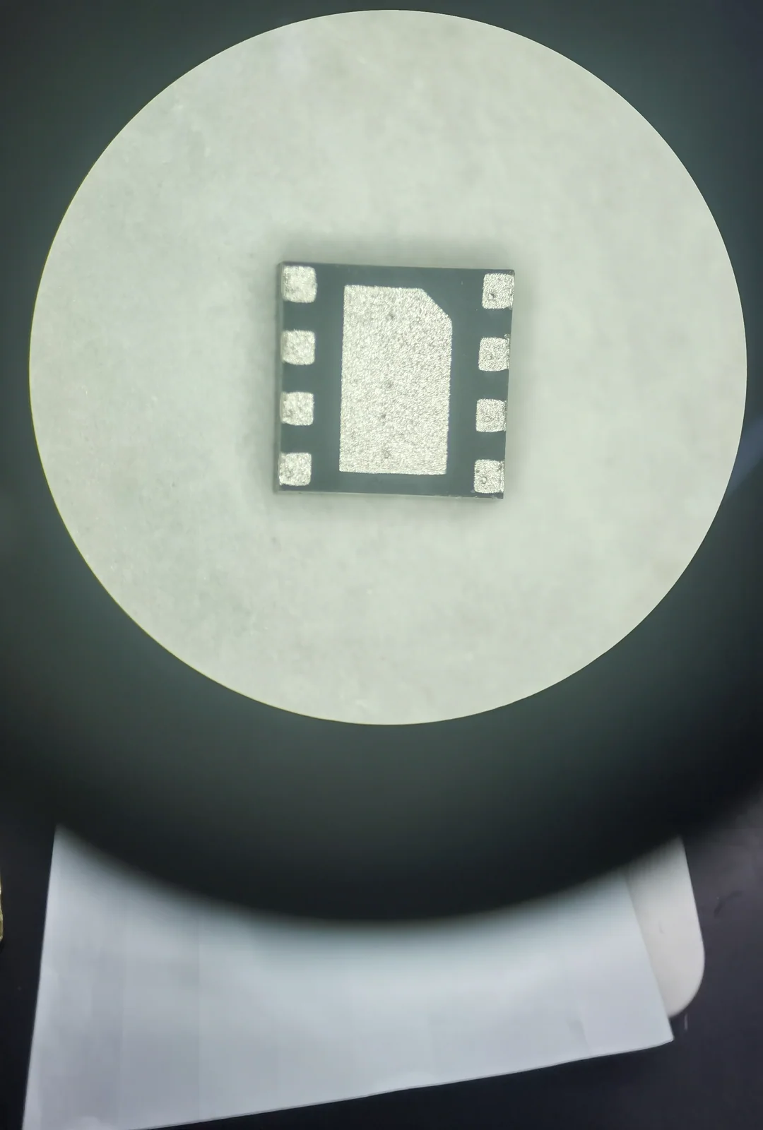
Microscope image of the underside of an eight-terminal package with a central metal pad.
Package underside showing the external terminals and central metal pad.

Packaged Samples

Packaged Samples & Visual Inspection

Packaged samples support board-level use and engineering evaluation. Package format, pin interfaces and sample preparation are coordinated before the next handoff.

TOMPW scope
TOMPW coordinated the package format, pin interfaces and sample preparation, with visual inspection records and handover documentation included as agreed.
Project stage supported
Packaged engineering samples prepared for board integration and further evaluation.
Semiconductor packaging
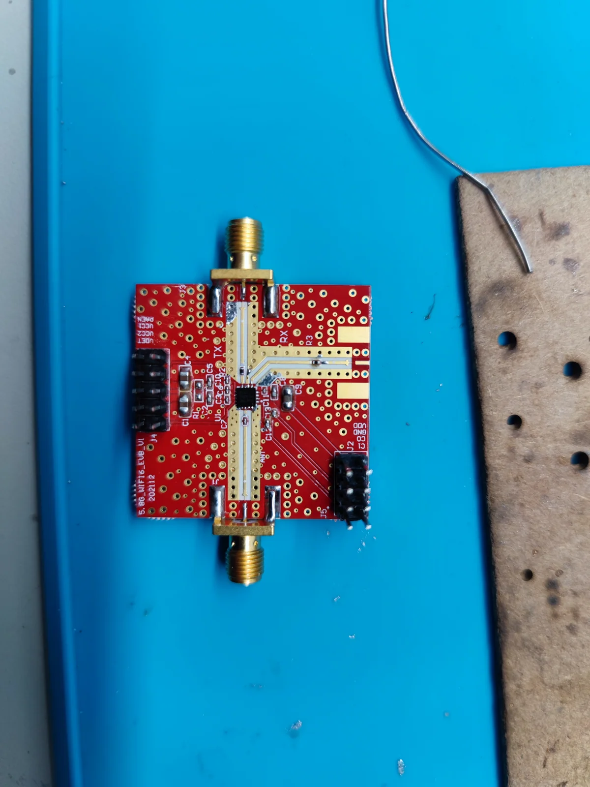
Red RF evaluation board with a central packaged device, two RF connectors and pin headers.
RF evaluation board with device, power, control and RF interfaces.

Board-Level Evaluation

RF Evaluation Board

An evaluation board provides RF connections, power and control interfaces for device bring-up and performance measurements, helping chip samples move into application evaluation.

TOMPW scope
TOMPW supported evaluation-board preparation and coordinated sample bring-up and RF measurement activities.
Project stage supported
A board-level evaluation platform connecting the packaged device to laboratory power, control and RF instruments.
PCB & evaluation-board support

Your Next Project

Plan the handoff from silicon to usable samples

Share your die or package format, sample quantity and evaluation requirements. We will define the assembly, test-interface and documentation scope around your project stage.