
Foundry profile
AWSCFoundry profile · process nodes · MPW shuttle windows · tape-out access
AWSC (Advanced Wireless Semiconductor Company) is a Taiwan-based pure-play GaAs foundry offering pHEMT and HBT processes for RF and microwave applications, including mobile and WiFi power amplifiers, VCSEL and integrated passive devices (IPD).
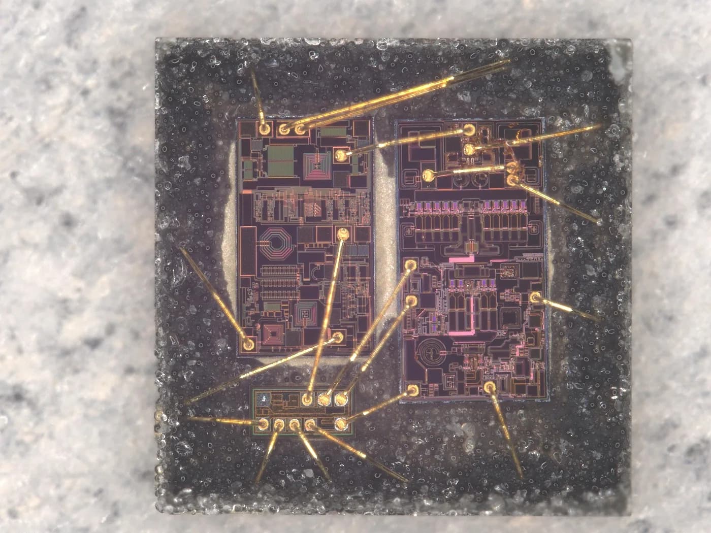
Representative imagery from semiconductor programs we have supported or analysed
Process Nodes
Technologies & Platforms
TOMPW Support Capabilities
Best For
Notes
- AWSC is a dedicated III-V (GaAs) foundry; TOMPW can coordinate MPW or dedicated GaAs runs.
- Suited to customers needing compound-semiconductor RF without owning a fab.
Plan the manufacturing route
Compare the process requirements with the package and test path before selecting a manufacturing route. Confirm the PDK, supplier acceptance, commercial terms and delivery scope in the project proposal.
Discuss AWSC for Your Program
Share the application, process requirements and target quantities. TOMPW will review feasibility and identify the access, package and test conditions to confirm for AWSC.
Email for a QuoteCOMMON QUESTIONS
Planning a AWSC project
Can TOMPW arrange MPW or shuttle runs at AWSC?
TOMPW reviews MPW, NTO and full-mask options for AWSC projects. Process acceptance, PDK access, run availability, quantities and delivery dates are confirmed for the specific project before booking.
What support does TOMPW provide beyond the wafer at AWSC?
TOMPW can scope packaging, final test, PCB and assembly work alongside the wafer requirements. The package route, responsible suppliers, test coverage and acceptance criteria are agreed in the project proposal.
How do I get a quote for a AWSC engagement?
Email market@tompwservice.com with the application, target process, program stage, volume and package or test needs. Start with non-confidential requirements; design files can follow through an agreed secure handoff.
RELATED FOUNDRY PROFILES
Other foundries teams compare AWSC with
RELATED SERVICES
Services that pair with a AWSC engagement
MPW / Fab Shuttle
Compare public shuttle windows across foundries, control first-silicon cost and move from tape-out planning to wafer delivery with one execution path.
Learn more →Full Mask / Production Foundry
Move validated designs into dedicated mask production with yield, volume and supply planning support.
Learn more →Semiconductor Packaging
Semiconductor packaging through external assembly and test providers, with TOMPW coordinating package selection, supplier review and assembly-to-test handoff.
Learn more →Test & Product Engineering
Connect CP, FT and reliability planning so packaged silicon is measurable, debuggable and ready for customer evaluation.
Learn more →Turnkey ASIC Solutions
Unify design support, tape-out, packaging, test, board work and delivery under one execution-facing partner.
Learn more →MPW / SHUTTLE ACCESS
Plan a AWSC MPW by process node
TOMPW coordinates multi-project wafer runs at AWSC across the nodes below. Open a node to see typical applications, what the run involves and how to book a shuttle slot.