
Knowledge Hub · Topic
Packaging & assembly guides
Package selection, thermal design, substrates and MSL, cost drivers and lead times — the packaging decisions that should be made before GDSI, not after.
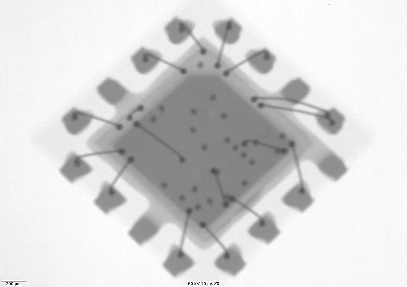
How to Select the Right IC Package: QFN, BGA, WLCSP, Flip-Chip and SiP
Package choice is a pre-tape-out decision that drives board cost, thermal, RF and yield. A practical framework for matching QFN, BGA, WLCSP, Flip-Chip and SiP to your design.
IC Package Thermal Management: What Actually Moves Junction Temperature
Thermal resistance is a system property, not a package property. What board design, TIM and airflow do to the number on the datasheet.
Package Substrates, Materials and MSL: What Buyers Should Ask
Substrate type, mold compound and moisture sensitivity determine cost, reliability and how you have to handle parts on the line.
Packaging Cost Drivers and Lead Times: Planning the Part Everyone Forgets
Assembly is often quoted late and underestimated. What actually drives package cost and where the weeks go.
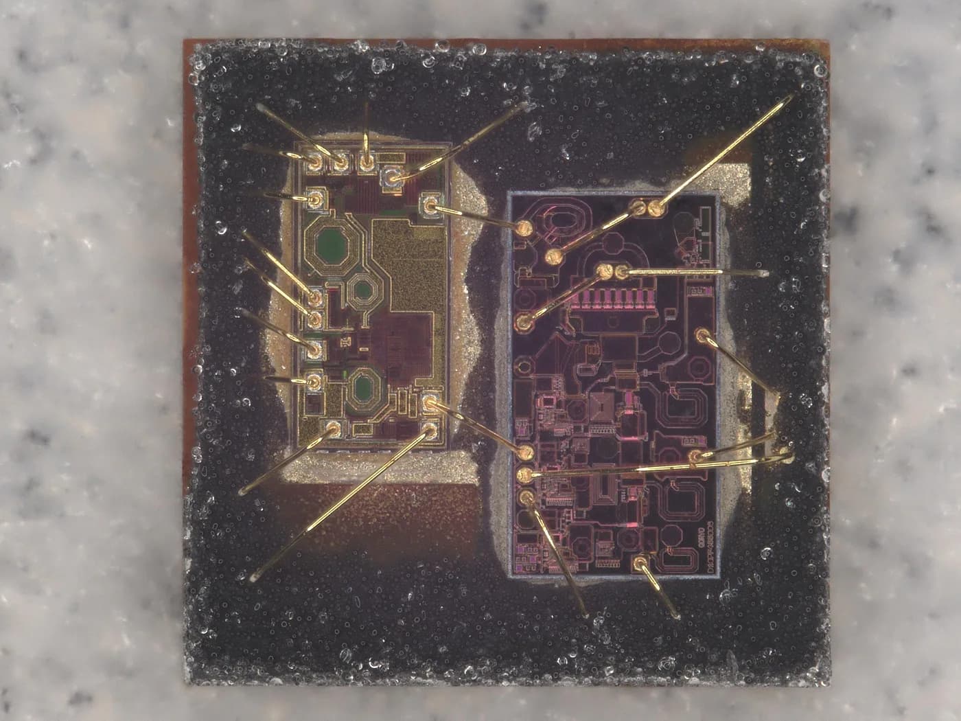
Wire Bond vs Flip-Chip: When Each Interconnect Wins
Wire bonding and flip-chip solve different interconnect problems. Compare cost, electrical, thermal and yield trade-offs to pick the right die-attach for your package.
Packaging and Test Checklist to Prepare Before Tape-Out
Packaging and test are where many programs lose momentum. This checklist explains what should be aligned before wafers come back.
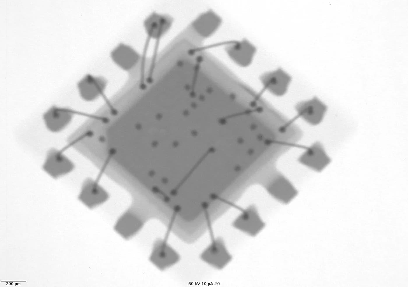
Advanced Packaging and Chiplets: What Changes for ASIC Programs
Chiplets and advanced packaging shift integration from the wafer to the package. Understand 2.5D, 3D, SiP and heterogenous integration, and when they beat a monolithic die.
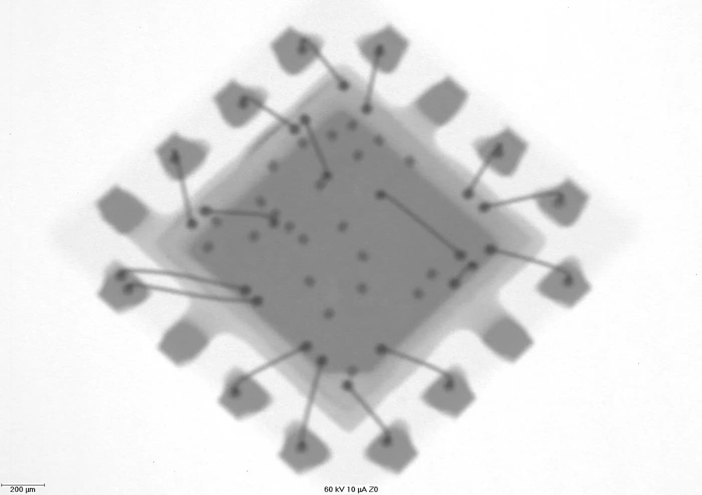
Packaging SiC and GaN Power Devices: What Is Different
Wide-bandgap SiC and GaN power devices stress packages in ways silicon does not. Compare thermal, parasitic, gate-drive and qualification needs for power packaging.
How to work through it
The order these decisions actually arrive in
01
Pick the package family on IO, power and thermal
Leadframe, QFN, BGA, WLCSP, flip-chip or SiP — the choice is constrained by IO count, power density, RF behaviour and board rules before cost enters the discussion.
02
Check the thermal path early
Junction temperature is set by the die attach, the pad and via design, the lid and the board — not by the package name on the drawing.
03
Fix substrate, materials and MSL
Substrate build-up, mould compound and moisture sensitivity level decide how the part must be stored, baked and reflowed in the customer's factory.
04
Read the cost drivers and the calendar
Assembly cost is driven by tooling, substrate, test and volume; the calendar is driven by substrate lead time and qualification slots.
05
Decide whether multi-die is worth it
2.5D, 3D, fan-out and SiP solve problems a monolithic die cannot — at a cost and a supply-chain complexity that has to be earned.
Which guide answers what
Pick by question, not by title
| Question | Read | What it settles |
|---|---|---|
| Which package fits my IO, power and RF constraints? | package selection guide | QFN, BGA, WLCSP, flip-chip and SiP against the real constraints of the design |
| Wire bond or flip-chip? | wire bond vs flip chip | Interconnect cost, parasitics, thermal path and yield |
| How do I keep junction temperature down? | package thermal management | Pad, via, lid and heatsink decisions that actually move the number |
| What does MSL do to my assembly flow? | substrate and materials msl | Moisture sensitivity levels, floor life, baking and dry packing |
| Where does assembly money and time go? | packaging cost drivers and lead times | Tooling, substrate, test and volume against the calendar |
| When does advanced packaging beat a bigger die? | advanced packaging chiplet | 2.5D/3D, fan-out and SiP against monolithic cost and risk |
Numbers to sanity-check against
Reference figures
Moisture sensitivity
JEDEC MSL 1 (unlimited floor life) through MSL 6 (bake before use)
Pb-free reflow
Classification profiles around 260°C peak for most plastic packages
Thermal lever
Board copper and via design often move RθJA more than the package choice
Qualification set
MSL preconditioning, TC, HTOL/uHAST and sometimes AEC-Q100 grade
Industry-wide reference points, not quotations. Your numbers depend on node, package, volume and test coverage — model them with the tools below.
EXECUTION
How TOMPW runs it
Semiconductor packaging through external assembly and test providers, with TOMPW coordinating package selection, supplier review and assembly-to-test handoff.
Semiconductor Packagingservice →