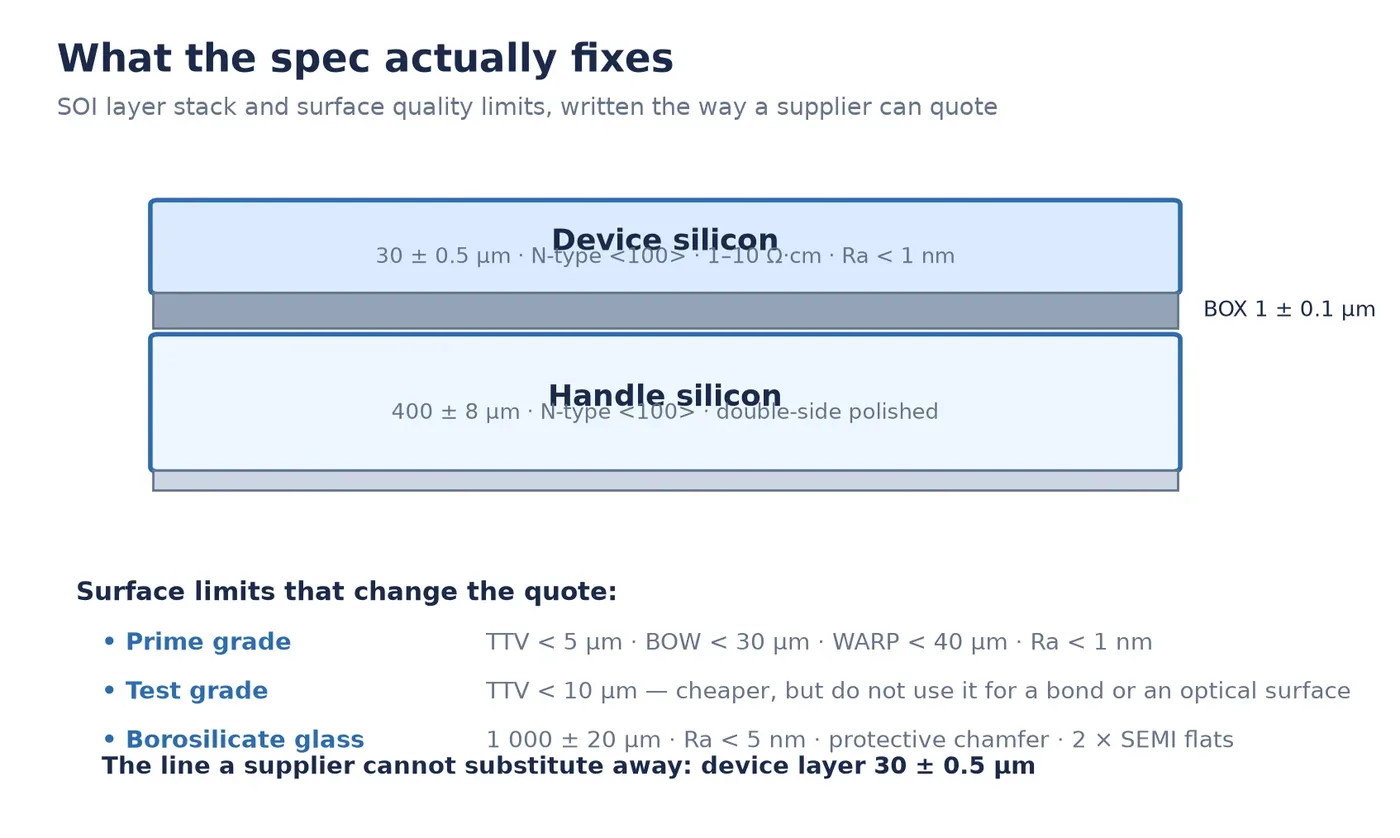
This is a real wafer map, not a textbook example. The layout file describes a 200 mm wafer carrying a product with a 12.24 mm × 15.24 mm die and a 240 µm scribe lane. The map places 127 gross dies per wafer.
The value of a real map is that it is a calibration point. Formulas for dies per wafer are approximations, and this one shows exactly how far off they can be on a large die.
The layout parameters
The map file records the following for the product, identified by the code 0EXH:
- Wafer diameter 200 mm, edge exclusion 3.5 mm, notch clearance 6 mm at the 6 o'clock position
- Die size 12.24 mm × 15.24 mm (186.5 mm²)
- Shot size 24.48 mm × 30.48 mm with a 2 × 2 reticle matrix
- Scribe (street) width 240 µm in both directions
- Gross dies per wafer: 127
What the standard estimate gives
The common closed-form estimate — effective wafer area divided by die pitch area, minus a perimeter correction — returns 136 for exactly these inputs. The real map places 127. That is about 7% fewer.
The gap has two named sources. The formula does not model notch clearance: 6 mm of unusable material at one point on the wafer edge removes dies that the circular effective-area calculation still counts. And it does not model reticle placement: a 2 × 2 reticle with a matrix shift places dies on a lattice whose interaction with the wafer circle is not the same as the ideal lattice the formula assumes.
On a small die the error is invisible in practice — a few dies out of several thousand. On a die this size, where each die is 186.5 mm² and represents a meaningful share of wafer cost, 7% is a real number in a quotation.
The dicing plan made it harder, not easier
The delivery plan for this wafer was not a single product. It called for seven different chip designs, fifty dies of each, cut from the wafer as blocks with the package shells handled separately. That kind of multi-product split changes the arithmetic again: the constraint is no longer how many dies fit, but whether the specific dies each product needs are in the usable region at all.
It also changes the conversation with the assembly line. Wafer grinding to a 12 mil target, dicing, and then holding package shells separate from dies are all normal requests, but each one is a parameter the assembly house needs in writing before the wafer arrives.
What to take from this
Treat a closed-form dies-per-wafer figure as an upper bound for large dies. For a 12 mm-class die on 200 mm, expect the real number to land 5–10% below the formula. If the number feeds a cost model or a quotation, either apply that margin or get the actual map — and the actual map is available earlier than most teams ask for it, because the foundry generates it at layout release.
Outcome
The dicing, grinding and packaging plan was executed against the real map rather than an estimate. The seven chip designs were cut, ground to the 12 mil target and supplied with their package shells as specified, and the customer's die-count and package requirements were met.