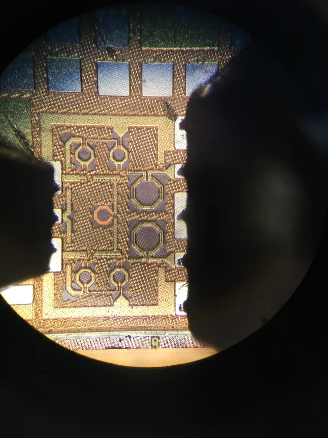
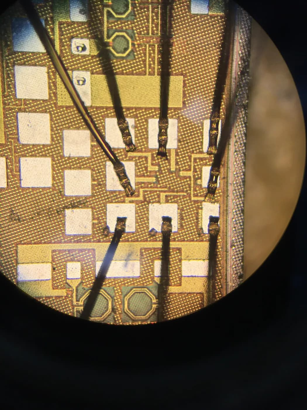
Two test insertions exist for a reason. Wafer sort happens while the die is still on the wafer and cheap to throw away. Final test happens after it has been packaged and is now worth real money.
Teams that treat CP and FT as the same test run twice pay for coverage they do not need. Teams that skip one of them ship escapes or scrap expensive packages.
Where Each Insertion Sits
Circuit probe (CP), also called wafer sort, runs at the foundry or a probe house right after wafer out. A probe card touches the die pads, the tester runs patterns, and failing die get inked or mapped out.
Final test (FT) runs at the assembly house after packaging. The part now has its real package parasitics, its real thermal path, and a handler instead of a prober.
- CP: bare die, probe card, wafer-level, pre-assembly
- FT: packaged part, load board and contactor or socket, post-assembly
- Some programs add a third insertion: system-level test (SLT)
What Wafer Sort Is Good At
CP is the cheapest place to kill a bad die, because you have not yet paid for the package. It is also the only place you get wafer-level spatial data, which is what makes yield learning possible.
Parametric failures, gross functional failures and most hard defect fallout show up here. Speed and accuracy limits measured at CP are indicative, not final, because the die is probed at a different temperature and through a different path.
What Only Final Test Can See
Packaging introduces failure modes that do not exist at CP: bond lift, wire sweep, die attach voids, mold stress, and package-induced parametric shift. None of these are visible before assembly.
FT is also where you run the tests that need the real thermal environment, the full IO at final load, and any calibration or trim that is more accurate after package. Speed binning is normally done here, not at CP.
The Cost Logic Behind the Split
The rule of thumb is simple: move anything that catches a substantial share of fallout as early and as cheaply as possible. Every die you reject at CP saves the full package and assembly cost of that unit.
The counterweight is that CP time is not free. A long CP program on an expensive tester can cost more per wafer than the packages it saves. The right split depends on your package cost, your expected CP yield and your tester rate.
- High package cost pushes coverage earlier, toward CP
- Low CP yield makes early screening more valuable
- Expensive CP time on advanced testers pushes coverage later
- Package-specific defects can only be caught at FT regardless of cost
A Workable Starting Split
A common pattern is a fast parametric and structural screen at CP, followed by full functional, speed and trim at FT. Structural patterns from scan are well suited to CP because they run quickly and catch a large share of hard defects.
For MPW and engineering runs the calculus changes: volumes are low, so the NRE of a dedicated CP program may not pay back. Many prototype runs go straight to FT with a light probe check, and move to full CP only when volume justifies it.