
Knowledge Hub
One content hub for visible progress and evergreen buying knowledge
This hub combines two things: dated updates that show current execution activity, and evergreen guides that answer recurring engineering and sourcing questions without getting stale after a week.
Latest dated update
July 9, 2026
Visible progress posts
3
Covered topics
13
Latest Updates
Dated execution signals customers can follow
These posts show ongoing activity across MPW, foundry, packaging and delivery topics, helping prospects see the site is current and helping GEO systems cite newer signals.
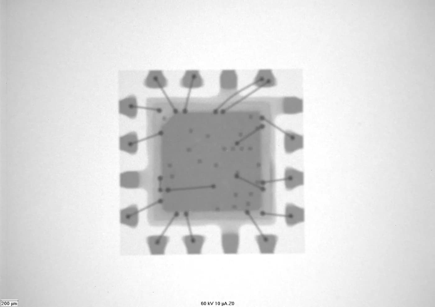
Why packaging lead times should be reviewed before MPW slot confirmation
Packaging is often treated as a post-tape-out task, but for many MPW programs the real schedule risk starts much earlier.
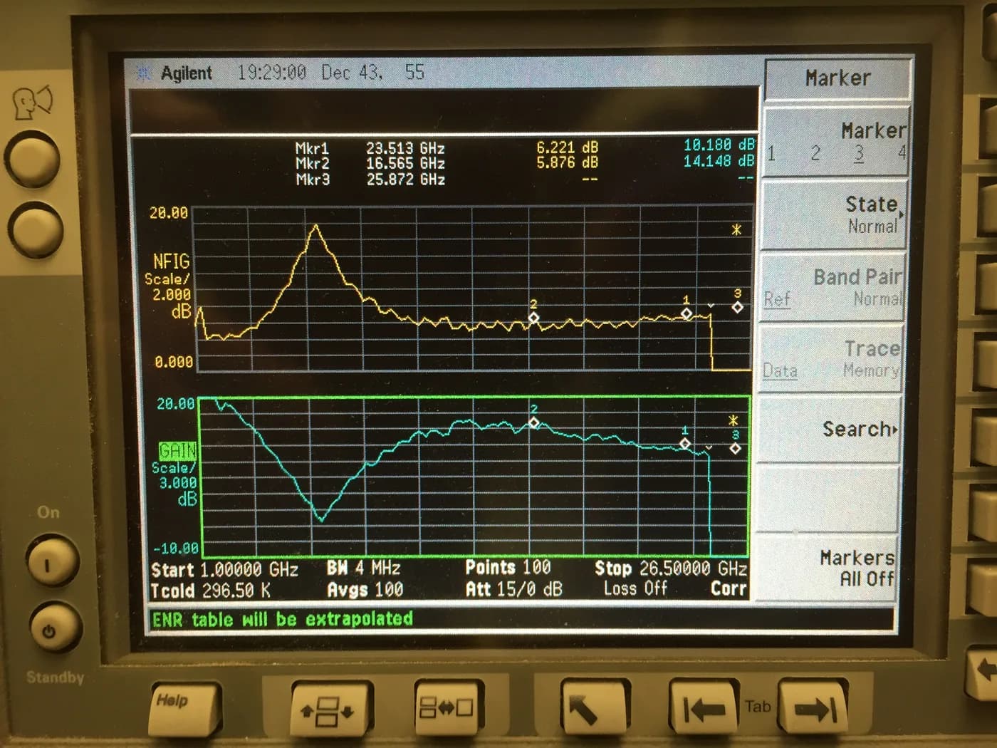
TSMC N3X Node Opens New MPW Window for AI Edge Prototyping
TSMC's N3X node is now accessible through MPW shuttle programs, giving AI edge chip teams a lower-risk path to advanced-node silicon validation.
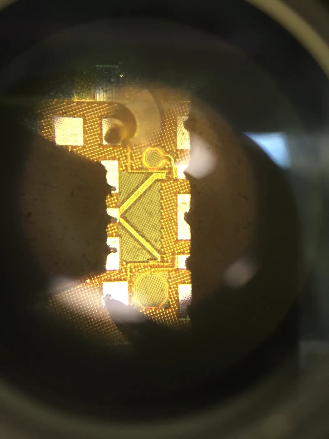
SMIC 28nm MPW: A Cost-Effective Path for IoT and Industrial ASIC Programs
SMIC's 28nm platforms remain one of the most cost-effective entry points for IoT and industrial ASIC programs that need mature yield and global supply chain access.
Evergreen Guides
Search-stable answers to common buying-stage questions
These pages target durable questions such as when to use MPW, how to choose a node and what to prepare in packaging or test before tape-out.
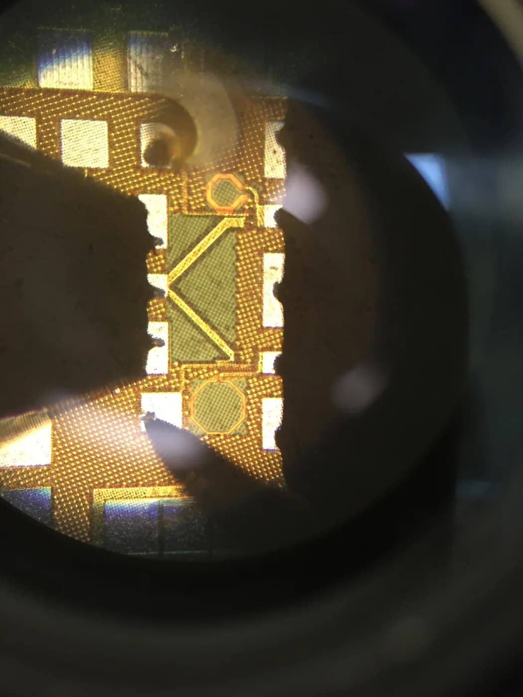
What Is MPW Service and When Should a Chip Team Use It?
A practical primer on MPW shuttle service, who it fits, how it lowers mask cost and where it sits in the broader tape-out path.
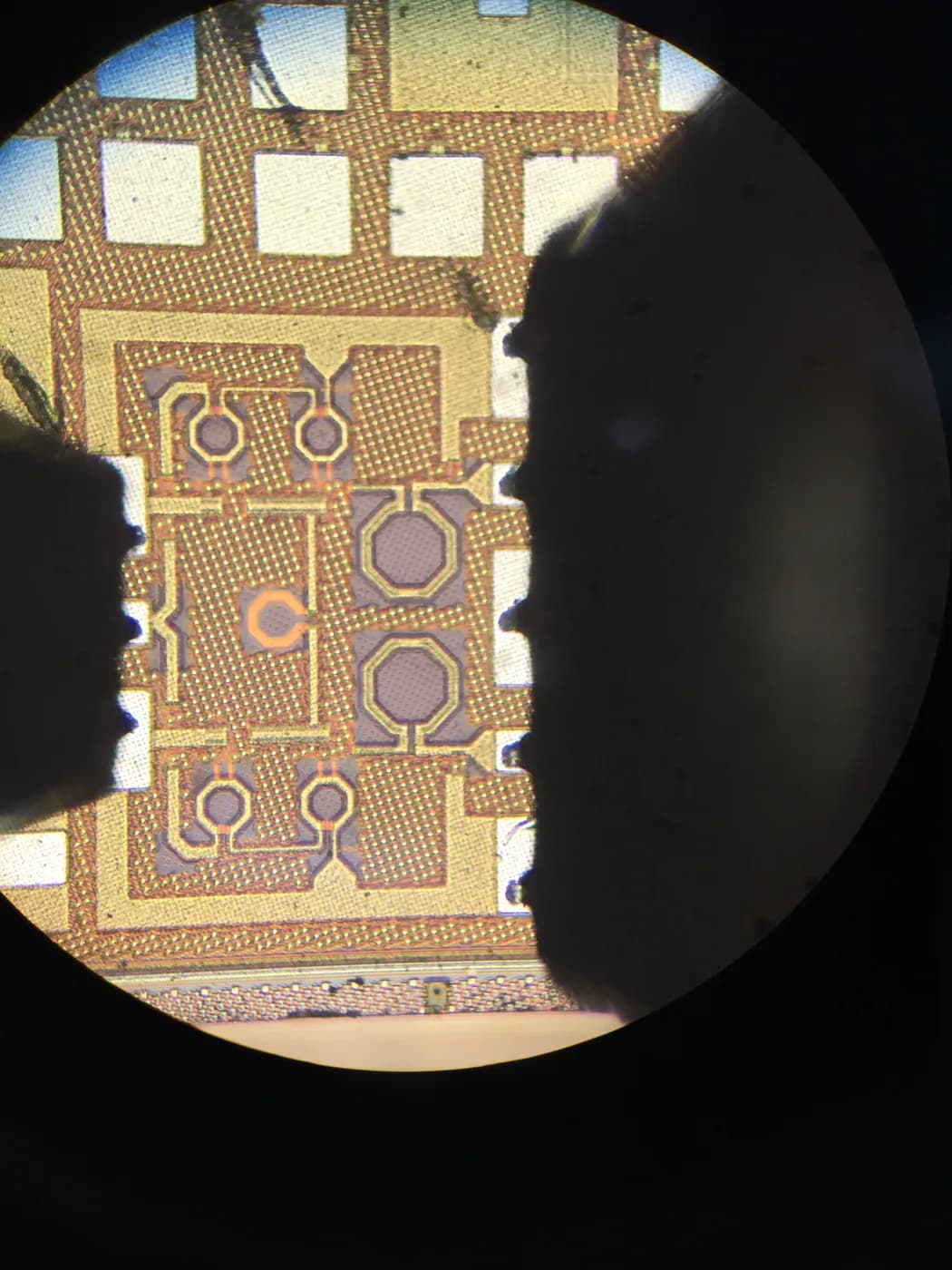
How to Choose the Right Foundry Node for an ASIC Program
Node choice is not only about shrinking geometry. It is a trade-off across cost, IP ecosystem, power, packaging and business timing.
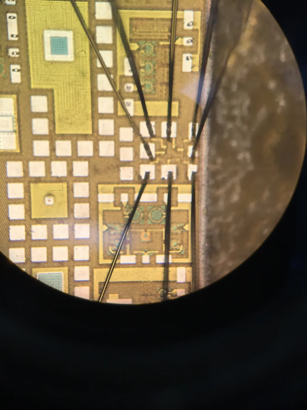
Packaging and Test Checklist to Prepare Before Tape-Out
Packaging and test are where many programs lose momentum. This checklist explains what should be aligned before wafers come back.
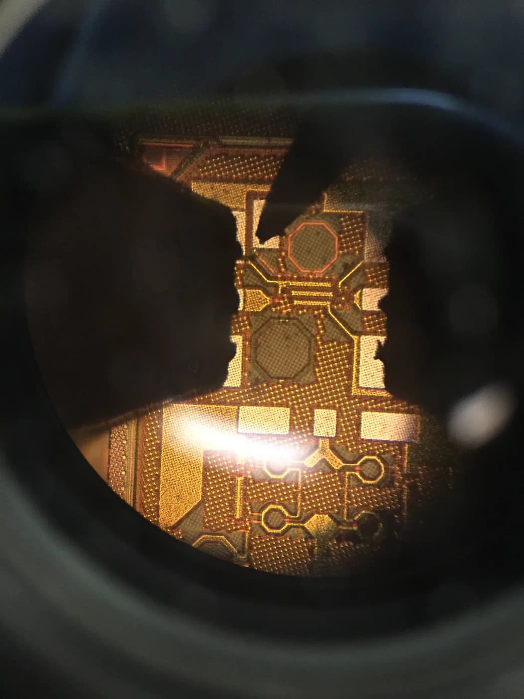
MPW vs Full Mask: Which Tape-Out Path Should You Choose?
MPW and full mask solve different problems. This comparison explains the cost, lead-time, volume and risk trade-offs so the right path is chosen early.
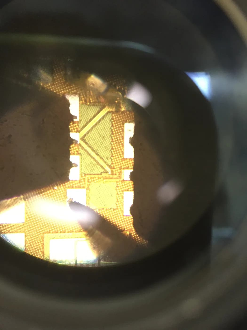
Process Node Comparison: From 180nm to 5nm and How to Choose
Node choice is not a single ladder. Mature and advanced nodes serve different products, costs and ecosystems across the 180nm to 5nm range.
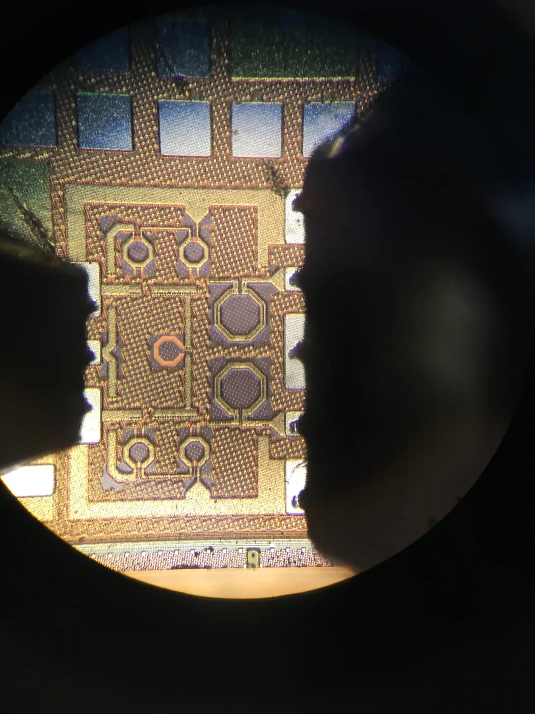
Process Technology Comparison: CMOS, BCD, BiCMOS, RF and FinFET
Beyond node size, the type of process technology decides what a chip can do. Compare CMOS, BCD, BiCMOS, RF and FinFET by function.
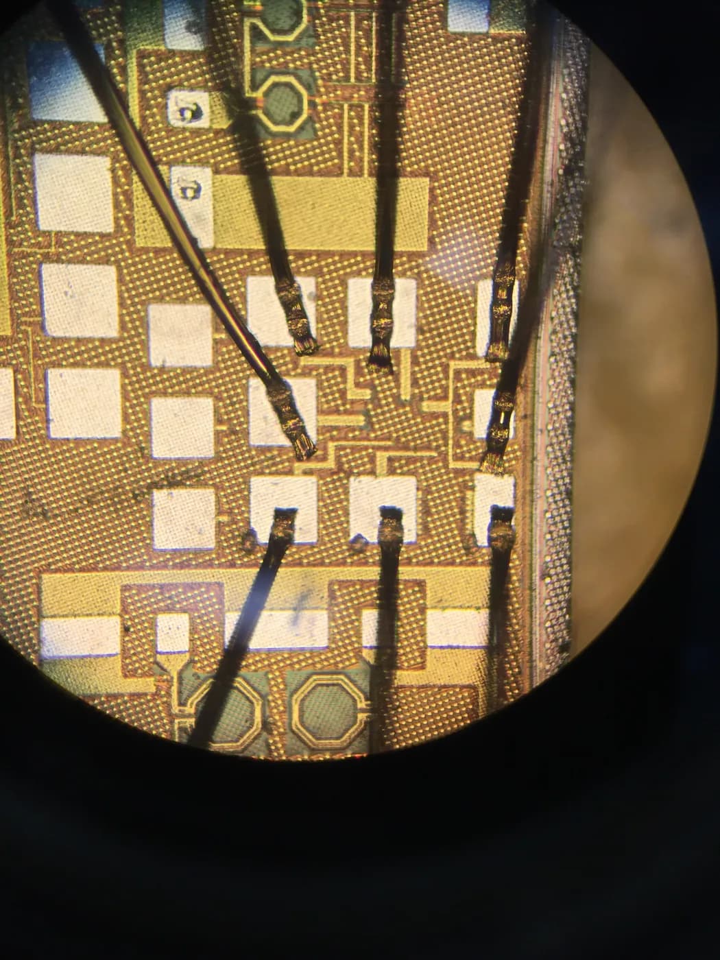
Foundry MPW Node Comparison: TSMC, SMIC, UMC and More
Each foundry offers MPW shuttle services at different nodes with different schedules, costs and access conditions. This comparison maps the landscape.
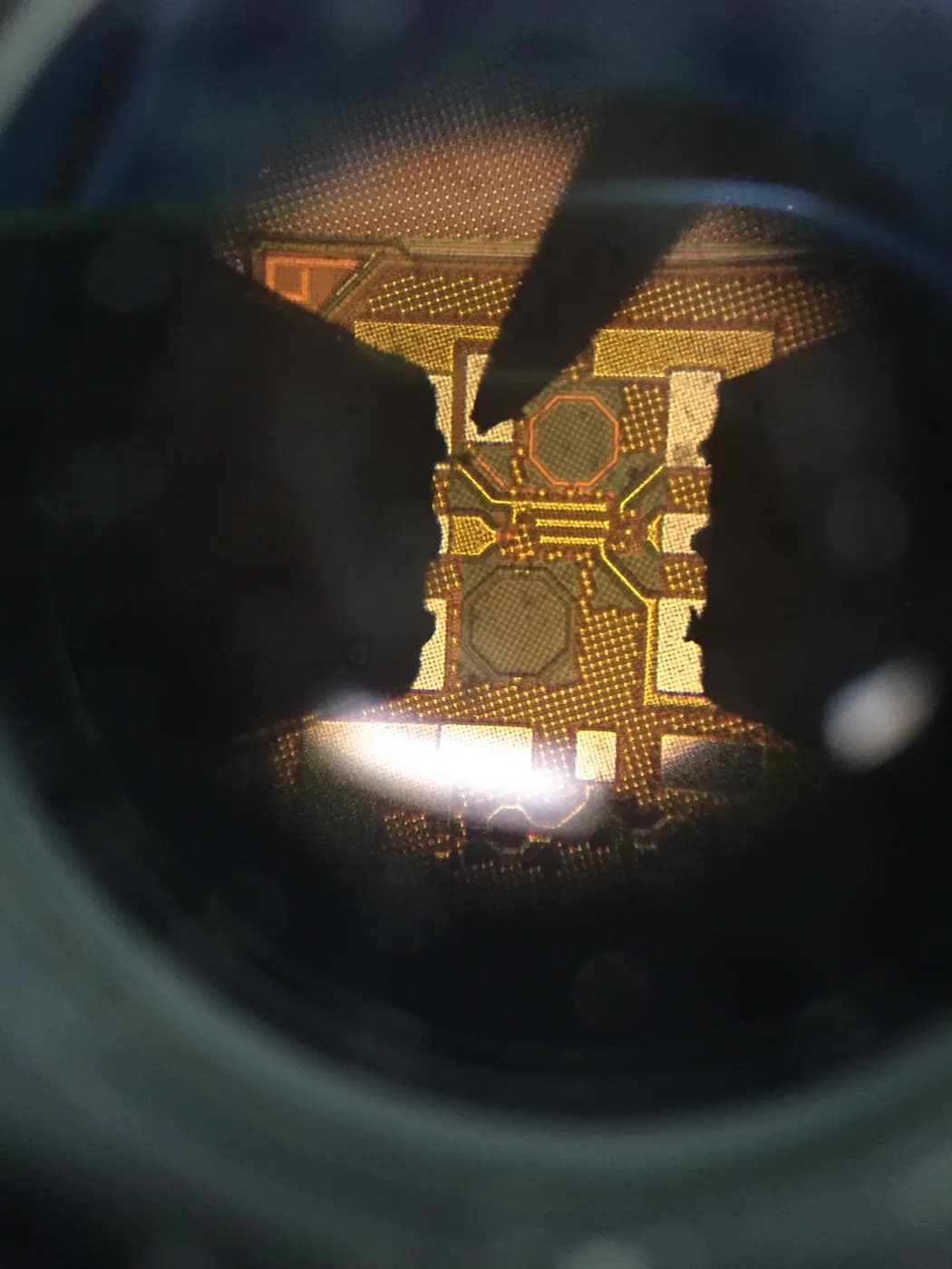
What We Learned Taping Out a 28nm Computing-in-Memory Chip
A field note from a real 28nm CIM tape-out: how the backend flow was structured, what surprised us, and the three decisions that protected the schedule.
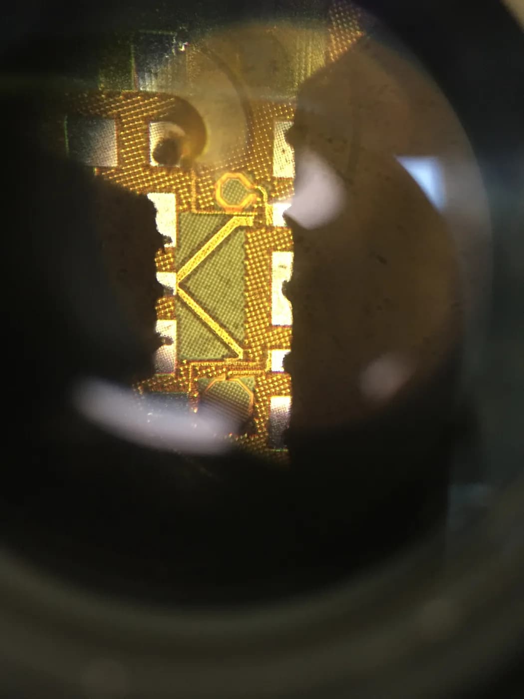
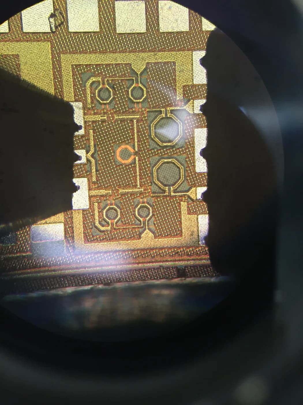
RF-SOI LNA: Three Tape-Outs in One Year
How a small RF fabless team ran three MPW shuttles for an LNA and RF switch in a single year — and what the die photography was used for.
Dual-Node TSMC CyberShuttle Enrollment for an Automotive MCU
A walkthrough of enrolling one automotive MCU program into TSMC CyberShuttle at two nodes simultaneously, and the AEC-Q100 prep that ran alongside it.
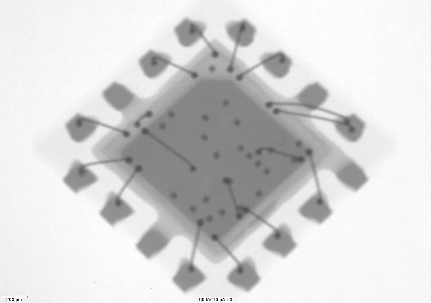
How to Select the Right IC Package: QFN, BGA, WLCSP, Flip-Chip and SiP
Package choice is a pre-tape-out decision that drives board cost, thermal, RF and yield. A practical framework for matching QFN, BGA, WLCSP, Flip-Chip and SiP to your design.
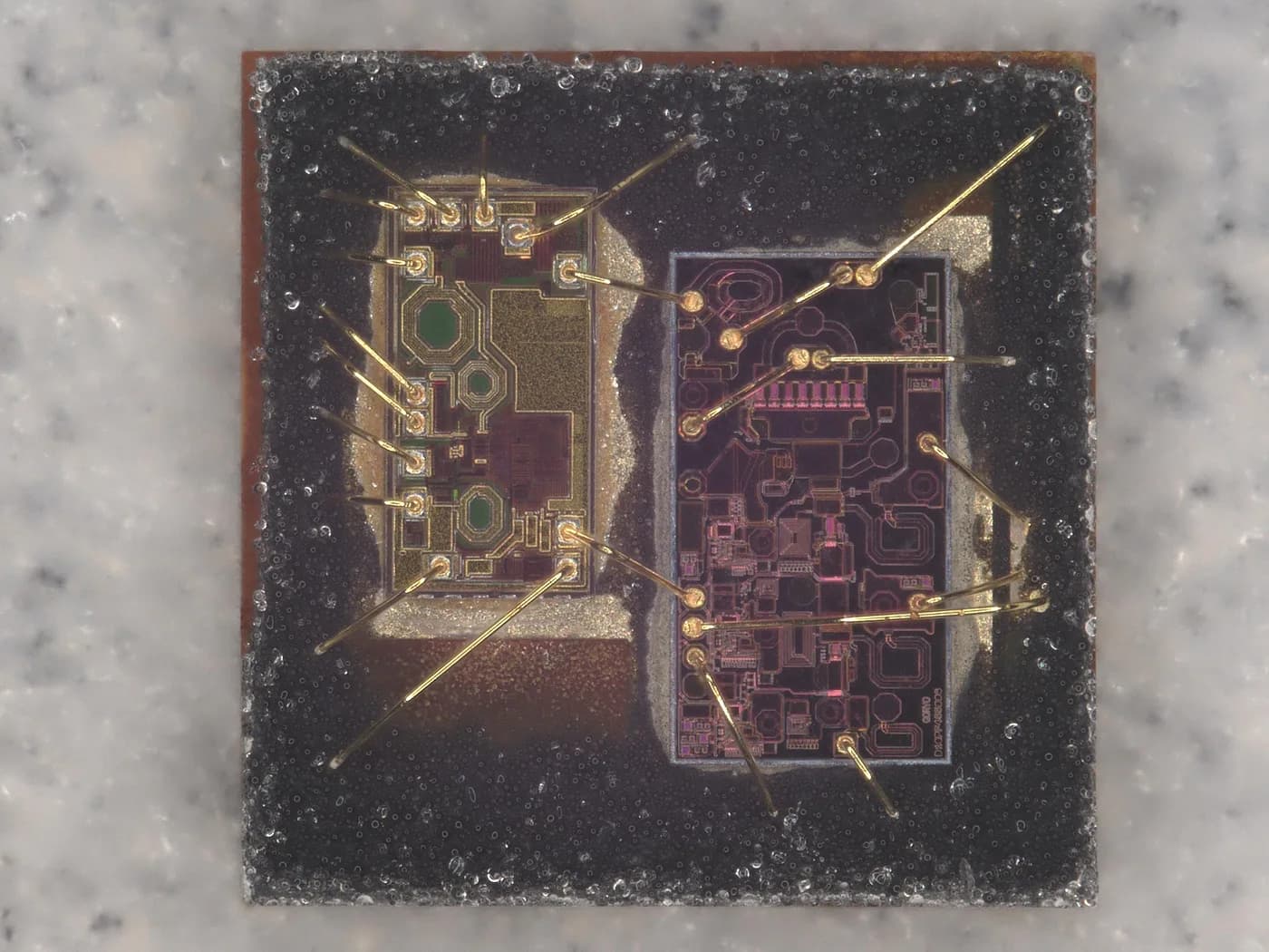
Wire Bond vs Flip-Chip: When Each Interconnect Wins
Wire bonding and flip-chip solve different interconnect problems. Compare cost, electrical, thermal and yield trade-offs to pick the right die-attach for your package.
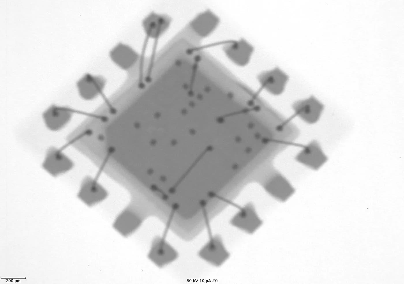
Advanced Packaging and Chiplets: What Changes for ASIC Programs
Chiplets and advanced packaging shift integration from the wafer to the package. Understand 2.5D, 3D, SiP and heterogenous integration, and when they beat a monolithic die.
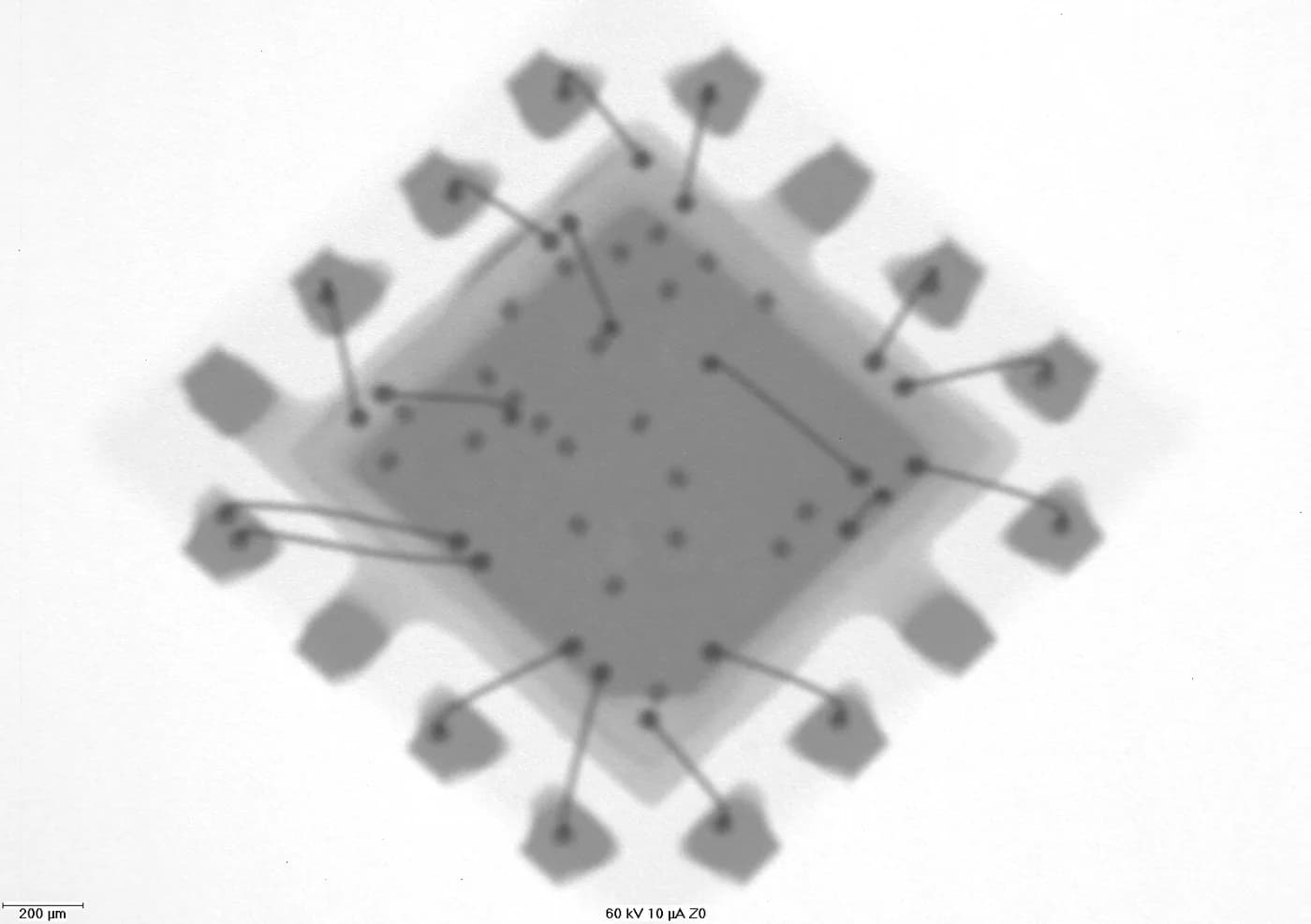
Packaging SiC and GaN Power Devices: What Is Different
Wide-bandgap SiC and GaN power devices stress packages in ways silicon does not. Compare thermal, parasitic, gate-drive and qualification needs for power packaging.
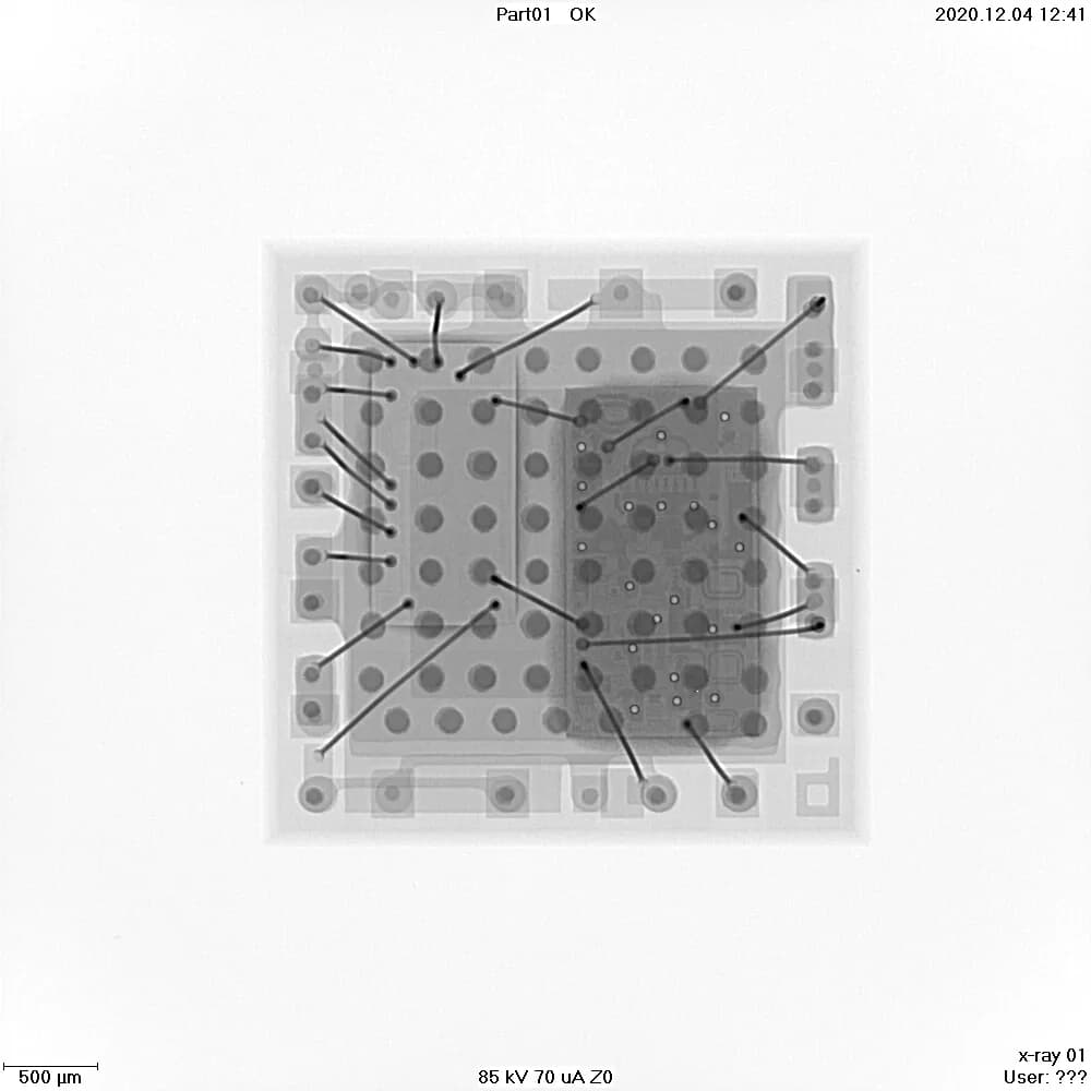
Reducing Test Cost: DFT, Yield and ATE Strategy
Test cost is paid on every die, good or bad. Learn how design-for-test, yield learning and ATE strategy cut cost per good unit without shipping risk.