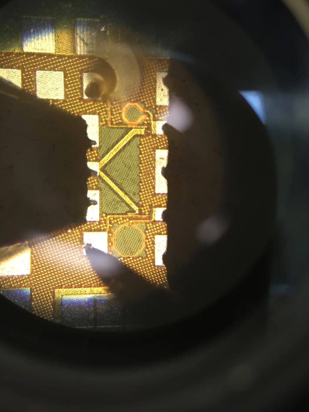
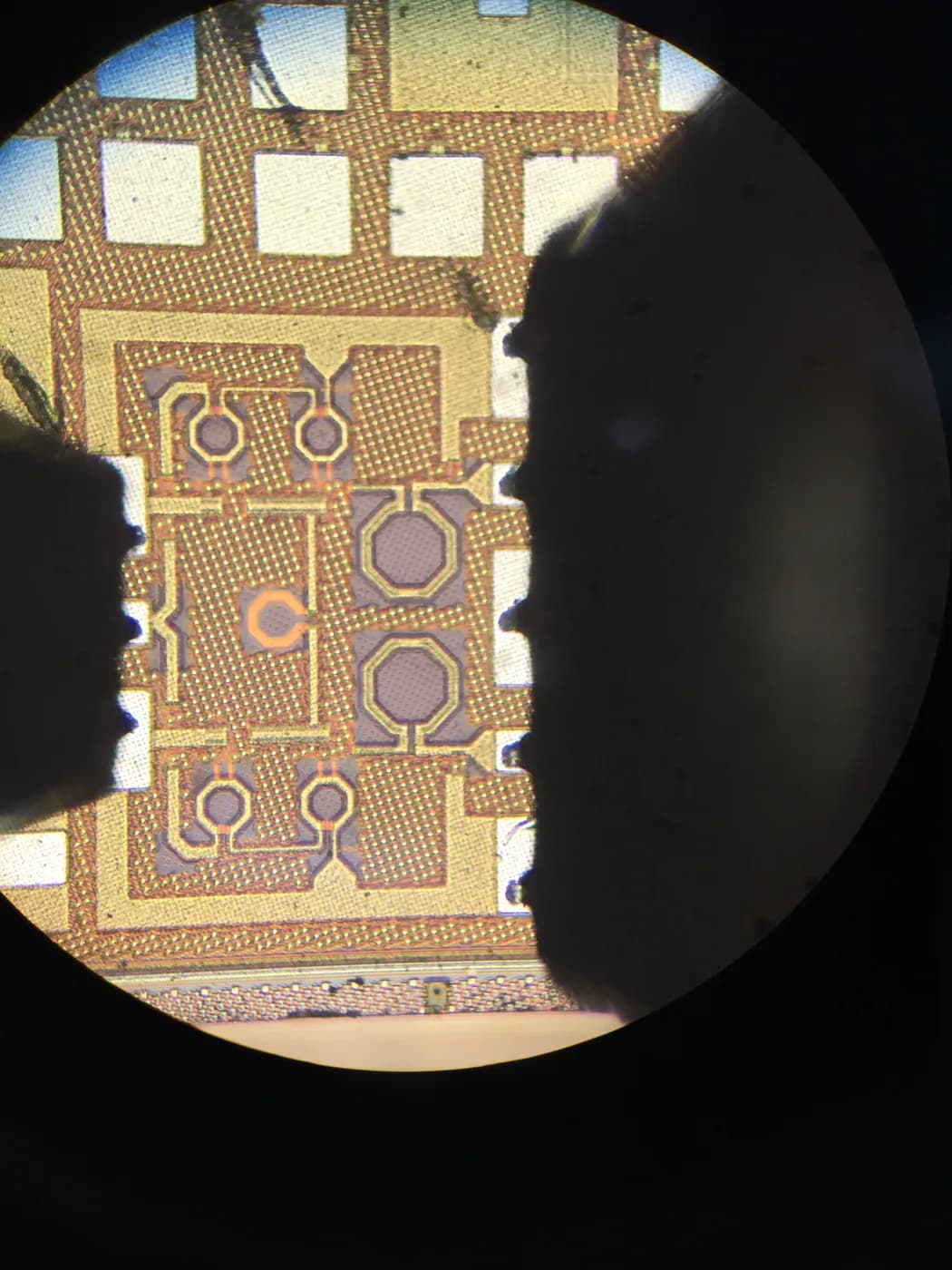
For decades, more integration meant a bigger, denser die. Advanced packaging changes the question: instead of putting everything on one wafer, you compose a system from multiple known-good dies in the package.
That shift has real consequences for cost, yield, time-to-market and supply strategy — and it is no longer only for the largest players.
What Advanced Packaging Actually Means
Advanced packaging covers 2.5D (dies on an interposer), 3D (dies stacked vertically), fan-out wafer-level and SiP approaches that combine logic, memory and passives.
The common thread is that integration happens at the package level, often using disparate process nodes for different dies.
- 2.5D: dies side by side on a silicon or organic interposer
- 3D: dies stacked with through-silicon vias
- Fan-out: reconstituted wafer with fine redistribution
- SiP: multiple dies plus passives in one component
Why Chiplets Improve Yield and Cost
A large monolithic die has low yield because any defect kills the whole part. Splitting it into smaller chiplets raises the yield of each piece and lets you bin and combine known-good dies.
It also lets you mix nodes — a mature, cheap node for analog and a leading node only where performance demands it.
When a Monolithic Die Is Still Better
For moderate complexity and cost-sensitive volumes, a single well-chosen node and package is simpler, cheaper and faster to qualify than a multi-die stack.
Advanced packaging only pays off when the integration, yield or mixed-node benefit exceeds its assembly and thermal-management overhead.
What Changes for Your Program
Multi-die programs need die-level test strategy, known-good-die handling and thermal planning that single-die programs do not.
The Package Selection Advisor and the Test Cost & Yield Calculator help scope the package and the test economics before you commit.