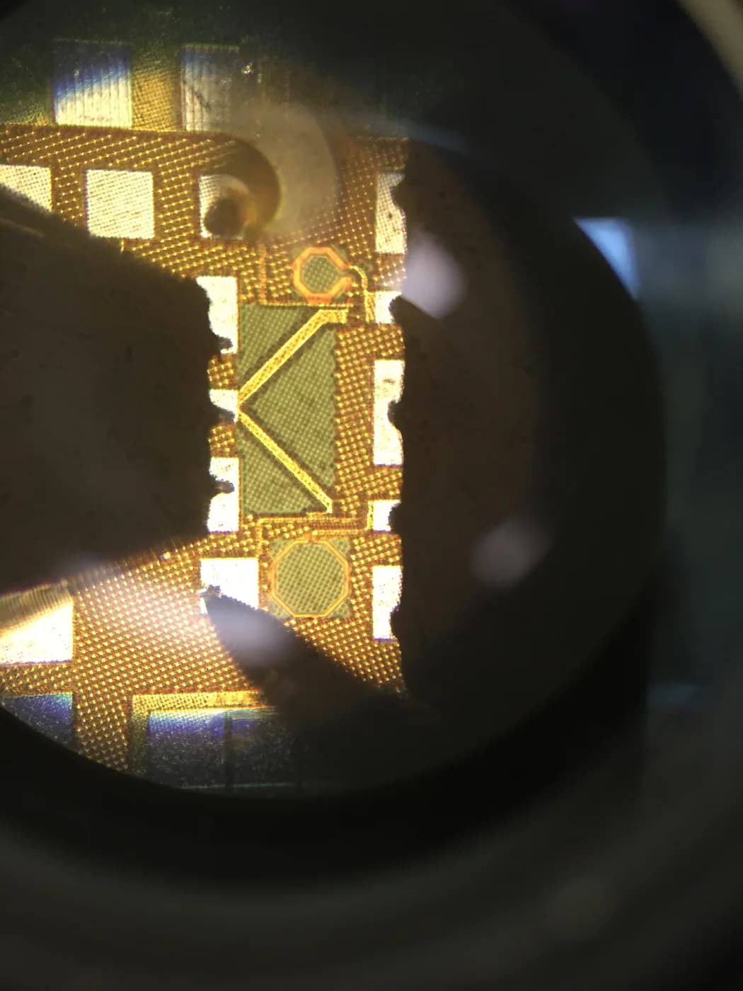
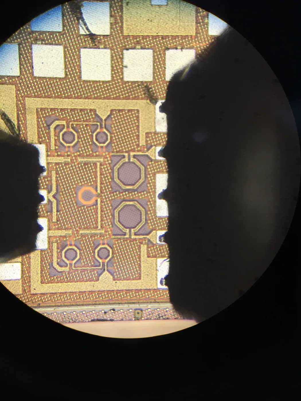
Two chips at the same node can do very different things because the underlying process technology is different. Node size is only one axis; process type decides function.
CMOS, BCD, BiCMOS, RF and FinFET each serve distinct purposes, and many products combine several of them.
Planar CMOS
Planar CMOS is the baseline digital and logic platform, dominant at mature and mid nodes where cost and density are well understood.
It is the default choice for digital logic, controllers and many mixed-signal designs where analog content is modest.
- Lowest cost and widest availability at mature nodes
- Excellent for digital logic and control
- Limited when large power devices or precision analog are needed
BCD (Bipolar-CMOS-DMOST)
BCD integrates bipolar, CMOS and DMOS power devices on one chip, enabling smart power ICs that combine control logic with power switching.
It is widely used in automotive, industrial and power-management products, and is offered by many foundries with qualified libraries.
- Combines control, analog and power on one chip
- Common in power management and smart power ICs
- Strong fit for automotive and industrial applications
BiCMOS
BiCMOS merges bipolar transistors with CMOS, adding high-speed and precision analog capability on top of digital density and low power.
It is a strong choice for high-speed transceivers, precision analog, RF and networking products where analog performance matters.
RF CMOS and RF SOI
RF CMOS brings wireless functions into standard CMOS where possible, while RF SOI is preferred for switches, tuners and antenna-front-end components.
These technologies target transceivers, connectivity and RF front-ends where linearity and isolation are critical.
FinFET and GAA
FinFET is a 3D transistor structure used from roughly 16nm and 14nm downward, offering better electrostatics, lower leakage and higher performance than planar at advanced nodes.
GAA, or nanosheet, extends this approach at 3nm and below as the leading-edge successor to FinFET.
- FinFET replaces planar at advanced nodes for power and performance
- GAA continues the scaling path below FinFET
- Both raise design and verification complexity
How to Choose Process Technology
Let function lead: digital logic points to CMOS or FinFET, power and smart power point to BCD, high-speed analog and RF point to BiCMOS or RF technologies.
Many programs mix technologies, for example CMOS logic with BCD power stages or BiCMOS RF blocks, so the choice is often a portfolio rather than a single pick.
Foundry availability for each technology varies, so process choice should be confirmed against the target fab's qualified offerings.