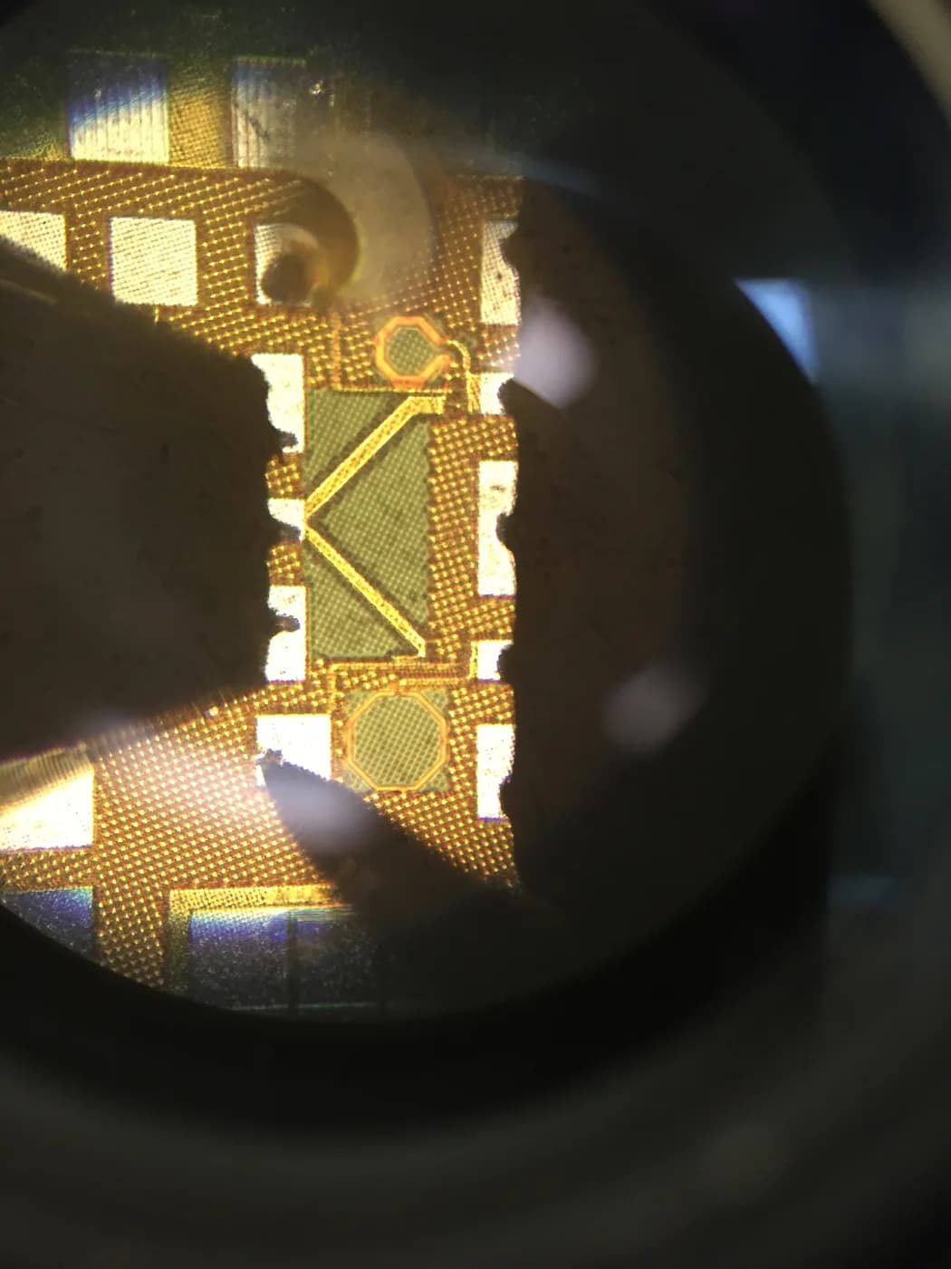
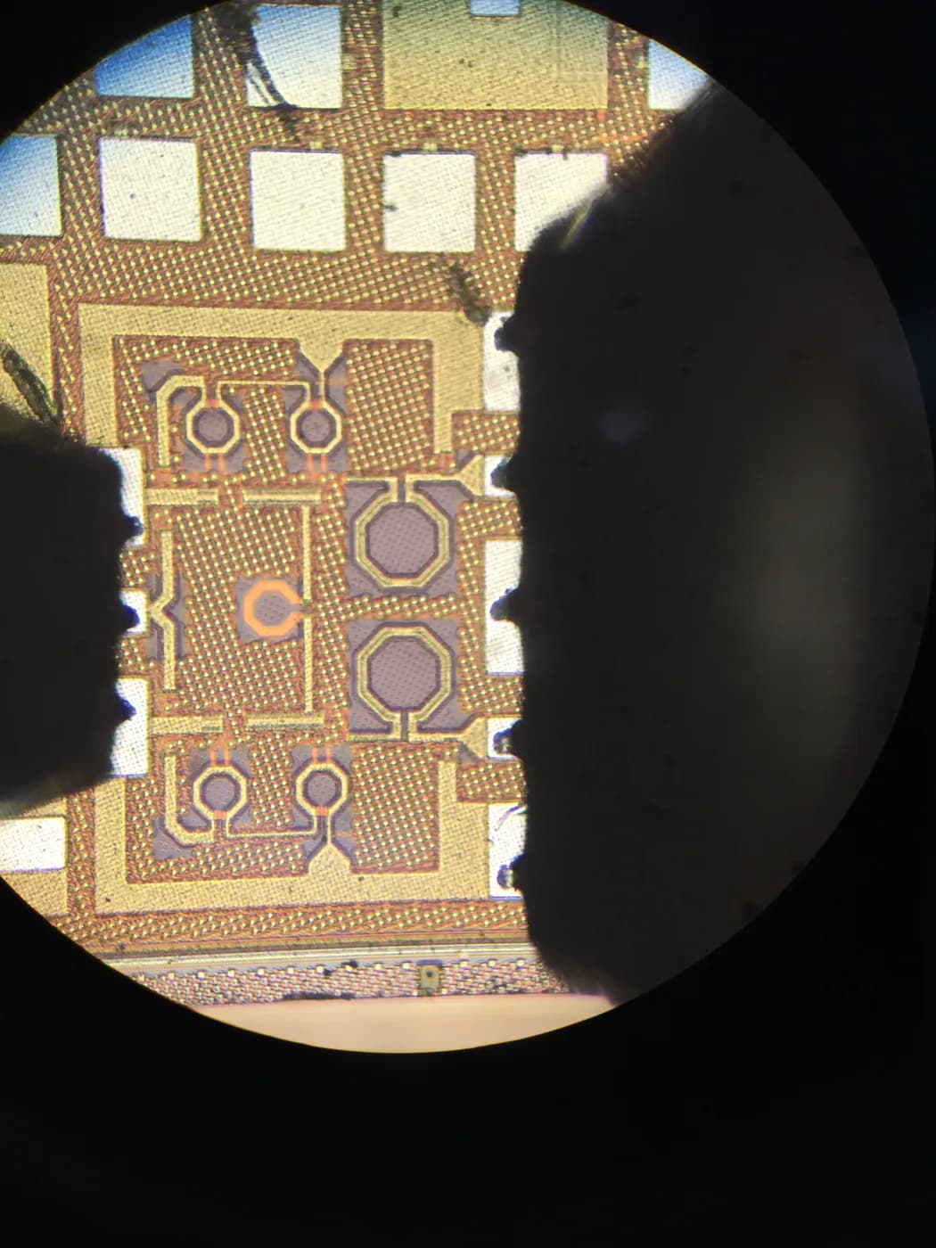
We are often asked what a real backend engagement looks like once the netlist is frozen. This note walks through a 28nm computing-in-memory (CIM) program we supported end to end, from netlist to clean GDSII sign-off.
Names and exact figures are generalized, but the engineering decisions are the ones we actually made — and the ones we would make again.
The program and its real constraint
The team had a working algorithm and a tight demo date tied to a funding milestone. The silicon did not need to be fast; it needed to be correct on first pass, because there was no slack to absorb a re-spin before the demo.
That single constraint shaped every downstream choice. We treated the backend not as a handoff, but as a schedule-protection exercise.
How we structured the backend flow
We ran the implementation and physical verification as overlapping stages rather than a linear chain, so that DRC/LVS issues surfaced early instead of at the end.
Key points in the flow:
- Floorplan driven by macro and memory placement, not left to the placer
- Early clock and power planning before detailed routing
- Incremental DRC/LVS checks after each major step, not only at the end
- A sign-off checklist owned by one engineer, reviewed by a second
What actually surprised us
The hardest issue was not timing — it was a subtle antenna rule violation that only appeared after fill insertion. Because we checked DRC incrementally, we caught it with days to spare rather than at tape-out.
The second surprise was how much schedule risk came from handoffs outside the chip: package outline and test plan had to be locked in parallel, or the wafer would have arrived with nowhere to go.
Three decisions that protected the date
First, we committed to a shuttle window before the design was final, which forced discipline on the critical path.
Second, we parallelized package and test planning with backend instead of queuing them after wafer completion.
Third, we kept one owner for sign-off accountability. Distributed sign-off is where silent slips hide.