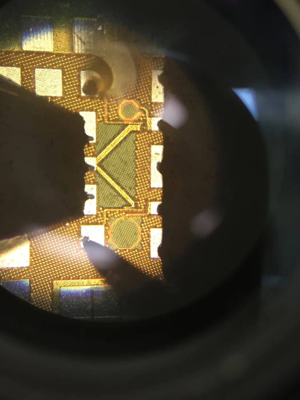
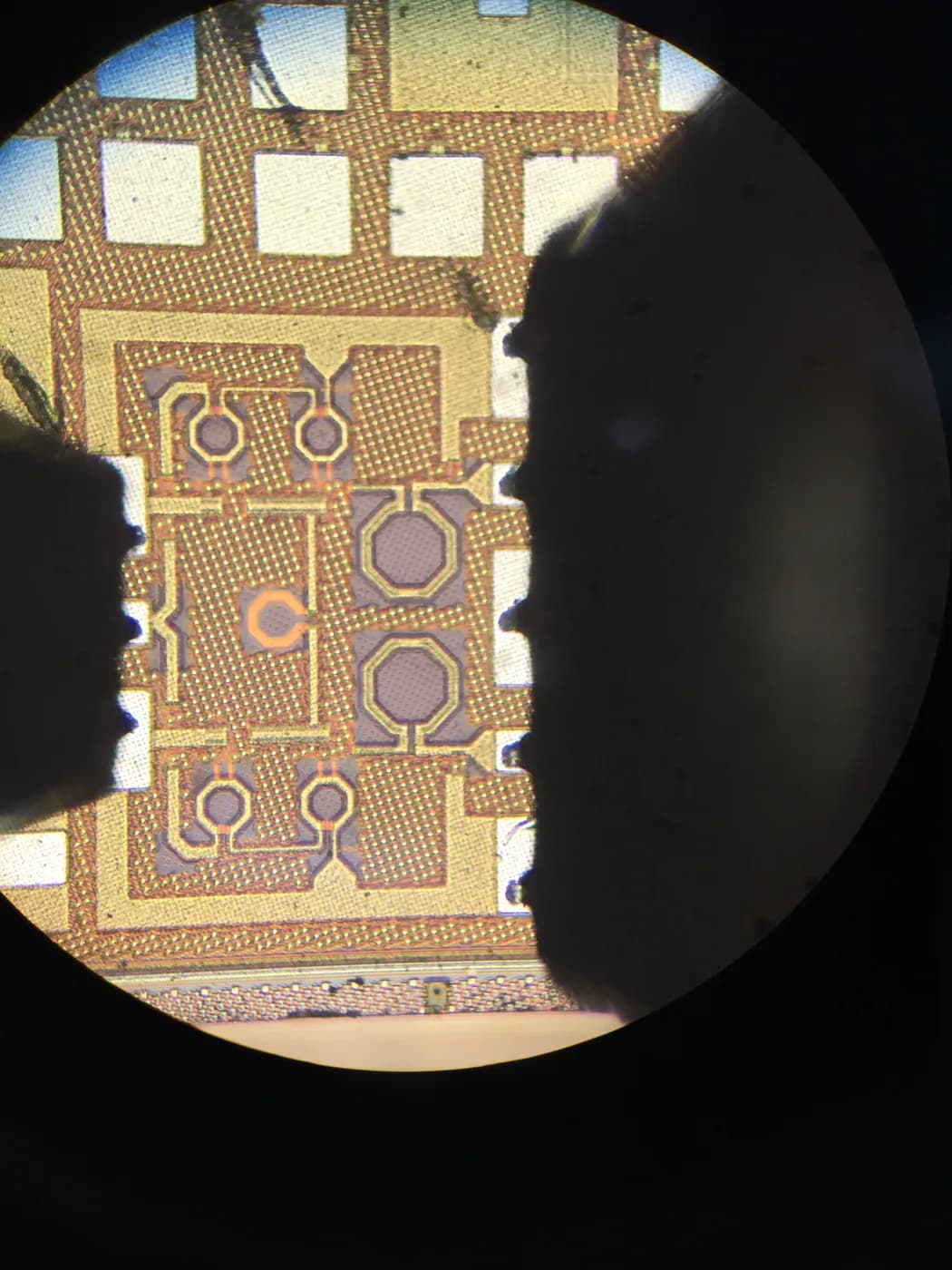
SiC and GaN move power electronics to higher voltage, frequency and temperature than silicon tolerates. That performance is won at the package, not just the die.
A package that is perfectly fine for a silicon MOSFET can wreck a GaN switch through parasitic inductance or kill a SiC module through thermal resistance.
Thermal Path Matters More
Wide-bandgap devices run hotter and switch faster, so the thermal resistance from junction to case is often the real limit on power rating.
Clip bonding, sintered die attach and direct-bonded copper substrates are common ways to pull heat out faster than a standard wirebond package allows.
- Low junction-to-case resistance is the rating ceiling
- Sintered attach and clip bonds beat wire bonds for thermal
- Direct-bonded copper substrates spread heat better
Parasitic Inductance Is the Enemy
Fast GaN switching makes package and layout inductance cause voltage overshoot and ringing. Minimizing loop area — sometimes with integrated gate drivers — is essential.
This is why many GaN parts ship in very low-inductance packages or even co-package the driver with the switch.
Gate Drive and Isolation
SiC gates need higher drive voltage and careful negative bias; GaN needs tight, fast gate control. The package must support that without adding noise or delay.
Proximity of the gate driver to the die reduces loop inductance, pushing some designs toward integrated or stacked-die solutions.
Qualification and Creepage
Automotive and industrial use demand creepage, clearance and humidity resistance that standard packages may not meet.
Qualification for SiC and GaN often runs longer and at harsher conditions than equivalent silicon parts, which should be planned before tape-out.