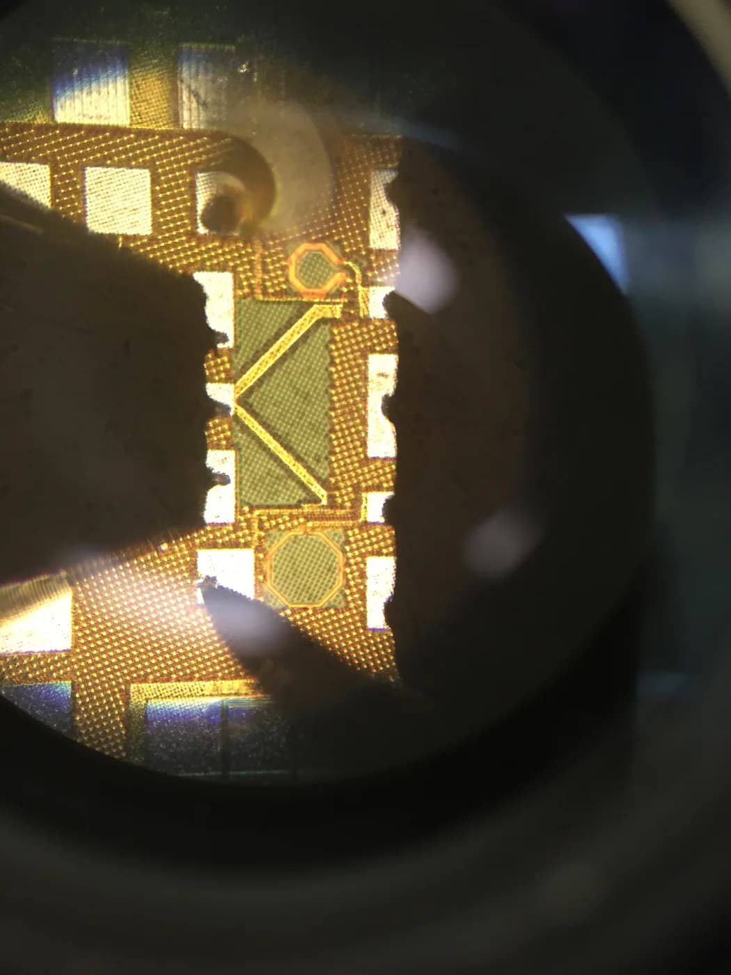
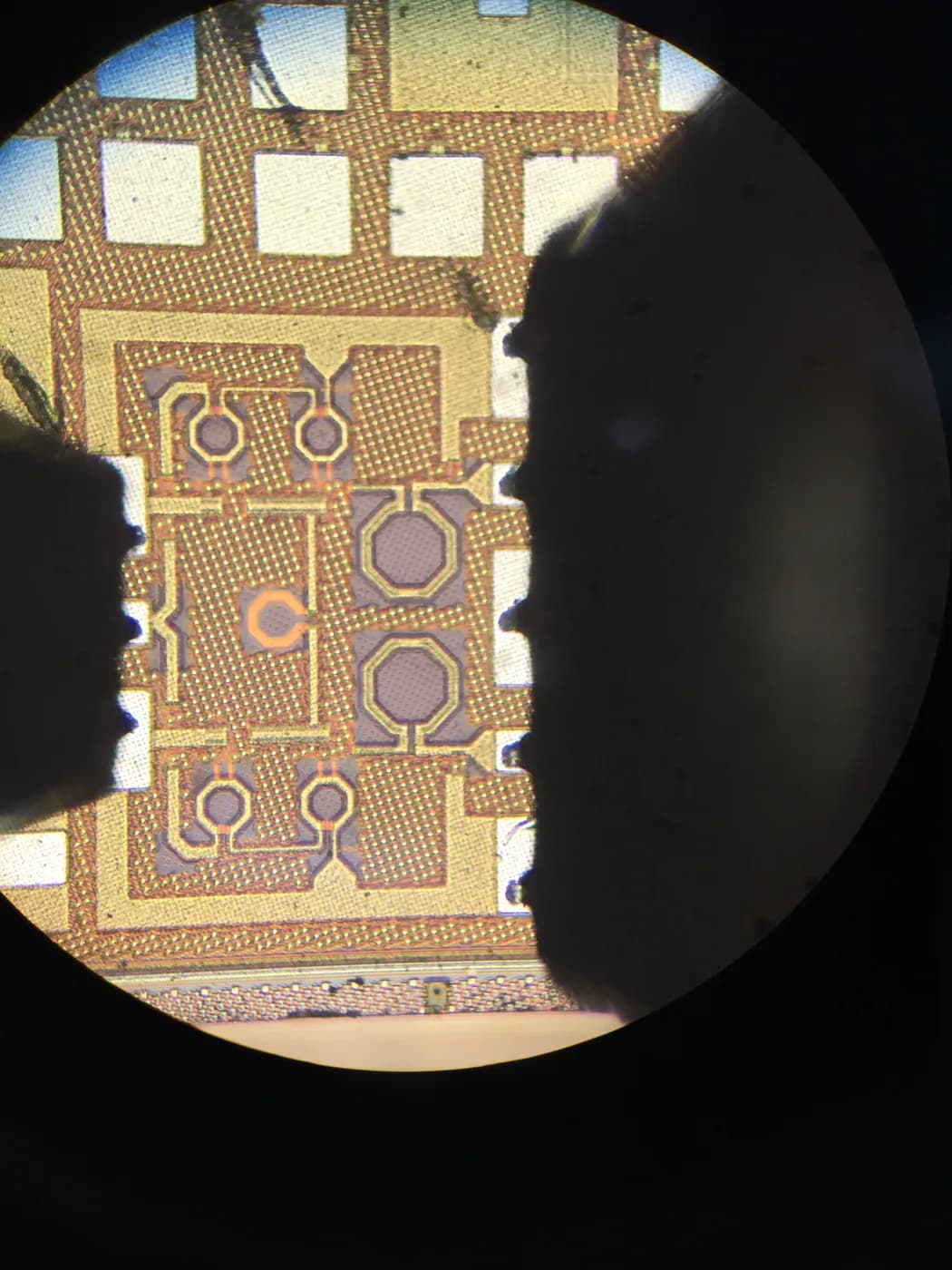
Die attach is not one technology. Wire bonding and flip-chip are the two dominant interconnect methods, and they trade off cost, performance and manufacturing complexity in opposite directions.
Choosing well means matching the interconnect to the signal, power and thermal demands — not defaulting to whatever the assembly house recommends first.
How Wire Bonding Works
Wire bonding connects die bond pads to the lead frame or substrate with thin gold or copper wires. It is mature, flexible and cheap per connection.
Its main drawback is parasitic inductance and resistance from the loop of each wire, which limits high-frequency and high-current performance.
- Lowest interconnect cost for low-to-moderate IO
- Tolerant of die and substrate variations
- Mature equipment and broad OSAT capacity
- Limited by wire inductance at RF and high current
How Flip-Chip Works
Flip-chip attaches the die face-down to the substrate through an array of solder bumps, giving a very short, low-parasitic path from die to board.
The short path delivers superior electrical and thermal performance, but the process needs bumped wafers, underfill and tighter substrate tolerance.
- Lowest parasitics, best for RF and high speed
- Excellent thermal path through the bump array
- Higher per-connection cost and process complexity
- Needs underfill and tighter substrate control
When Wire Bond Wins
For low-to-moderate IO, cost-sensitive and power-or-mixed-signal devices that do not push RF or thermal limits, wire bonding is usually the rational choice.
It also suits prototypes and low-volume runs where bumped-wafer setup cost is hard to justify.
When Flip-Chip Wins
For high IO, high frequency, high current or high thermal loads, flip-chip pays for itself through performance and reliability.
Advanced nodes and high-bandwidth devices almost always require flip-chip because wirebond parasitics would dominate the link budget.