CHIPS Act Impact: What the US Semiconductor Funding Law Means for MPW Programs and Design Teams
Signed into law in August 2022, the CHIPS and Science Act represents the most significant US government intervention in semiconductor manufacturing policy in decades.
With USD 52.7 billion in subsidies and tax incentives aimed at onshoring semiconductor fabrication, the law sends a clear signal about US priorities in advanced chip production — and creates ripple effects that extend well beyond US borders.
For MPW program participants and design teams, the relevant questions are: How does CHIPS Act funding affect shuttle availability? Do export control frameworks change? And what does this mean for programs that rely on US-designed IP or US-headquartered foundry services?
Key Provisions Relevant to MPW and Prototyping Programs
While much of the public attention focused on the large-scale fabrication incentives (USD 39 billion in manufacturing grants), several provisions of the CHIPS Act have direct or indirect relevance to MPW shuttle operations and prototype-focused ASIC programs.
The National Defense Technology Acceleration (NDTA) provisions include funding for semiconductor workforce development and prototyping infrastructure that could expand domestic MPW capacity over time.
Additionally, the guardrail provisions — restricting companies that accept US CHIPS funding from expanding advanced-node capacity in 'countries of concern' for 10 years — create new strategic considerations for foundries that operate both US and international fabs.
- USD 52.7 billion total: USD 39B manufacturing grants + USD 13.2B R&D + tax credit
- Guardrails: Recipients restricted from expanding advanced-node capacity in designated countries for 10 years
- NDTA funding includes prototyping infrastructure — potential future MPW expansion in US
- Workforce development funding may ease talent bottlenecks that currently delay tape-outs
Impact on Foundry Capacity and Shuttle Calendars
In the near term (2022–2024), the primary effect of CHIPS Act on MPW programs is indirect: as major foundries announce US fab construction plans in response to incentive structures, capital allocation and capacity planning priorities shift.
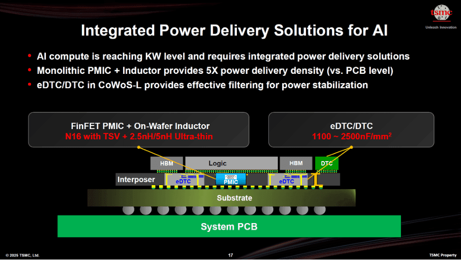
TSMC's Arizona facility (N4/N5 process, announced prior to CHIPS Act passage but accelerated by it), Intel's expanded IDM 2.0 foundry services, and potential new entrants into US-based advanced-node manufacturing all represent capacity additions that will take 3–5 years to come online.
During this transition period, MPW shuttle availability at existing facilities (primarily in Asia) continues to operate on existing calendars, but design teams should monitor for any scheduling adjustments as foundries rebalance engineering resources toward US construction projects.
- Near-term (2022-2024): Minimal direct impact on existing Asian-fab MPW shuttle calendars
- Medium-term (2024-2027): Potential capacity relief as new US fabs come online
- Long-term: Potential expansion of US-based MPW shuttle options for eligible programs
- Monitor: Foundry engineering resource allocation between US projects and existing operations
Export Control Considerations for International Teams
The CHIPS Act is accompanied by tightened export control frameworks administered by the US Bureau of Industry and Security (BIS).
For design teams — particularly those in regions subject to enhanced scrutiny — the practical implication is that node-level access, IP licensing and foundry engagement may face additional compliance checkpoints compared to the pre-CHIPS Act environment.
This does not necessarily mean that MPW participation becomes impossible for non-US teams, but it does mean that due diligence on export classification, end-use certification and technology transfer controls should be factored into program planning timelines.
- Enhanced BIS reviews for advanced-node (sub-14nm) technology transfers to certain regions
- 'Foreign direct product rule' expansions may affect where designs using US-origin IP can be manufactured
- End-use and end-user certifications may be required for some MPW program participations
- Recommend engaging export compliance counsel early for programs involving sensitive applications
Practical Guidance for ASIC Teams Post-CHIPS Act
For design teams outside the United States working on MPW-based ASIC programs, the post-CHIPS Act environment requires slightly more upfront planning but does not fundamentally change the viability of the MPW path.
Key recommendations: verify export classification of your target node and IP before committing to a shuttle window; maintain documentation of end-use and end-user credentials; consider diversifying across foundries with different jurisdictional profiles; and build relationships with service providers who understand both the technical and regulatory dimensions of cross-border semiconductor programs.
- Check export classification early — do not assume pre-CHIPS Act rules still apply unchanged
- Document end-use clearly — vague descriptions invite compliance delays
- Consider multi-foundry strategy — diversification reduces concentration of regulatory risk
- Factor 2–4 additional weeks into planning for potential compliance review cycles
- Work with partners experienced in cross-border semiconductor services (like TOMPW)