FinFET Process Selection: A Practical Comparison of 7nm and 16nm/12nm for ASIC Programs
By 2018, FinFET technology had moved well beyond its initial introduction and was available across a range of nodes from 16nm down to 7nm at major foundries.
For ASIC teams evaluating which node to target, the decision is rarely as simple as picking the most advanced option. Power, performance, area, cost, IP availability and MPW access all play into a matrix that looks different for every program.
Where 7nm Stands in 2018
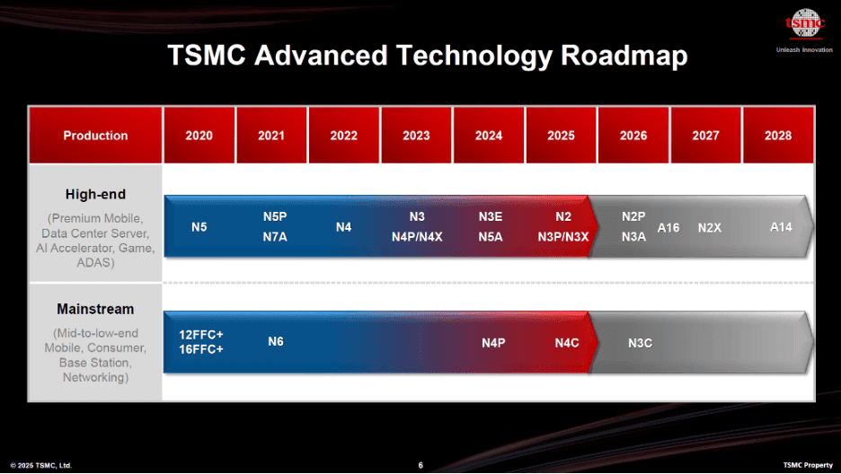
TSMC's 7nm (N7) process entered volume production in 2018, offering a genuine density and power improvement over the preceding 16nm/12nm FinFET generations.
Early 7nm products were concentrated in high-performance computing, smartphone applications processors and networking ASICs where the per-transistor power savings justified the higher wafer cost and more complex sign-off flow.
For general-purpose ASIC programs, however, 7nm in 2018 still carried meaningful premiums in mask cost, IP licensing and design tool requirements compared to 16nm/12nm.
- 7nm offers approximately 25–35% speed gain or 35–45% power reduction vs 16nm at iso-performance
- Wafer cost at 7nm is roughly 1.8–2x higher than 16nm at equivalent volumes
- IP ecosystem at 7nm is narrower than at 16nm — fewer third-party IP vendors have qualified cores
- MPW shuttle frequency at 7nm is lower and wait times longer than at 16nm
The Case for 16nm/12nm FinFET
Despite being several generations behind the leading edge, 16nm and 12nm FinFET processes remain highly competitive for a broad range of applications in 2018.
The key advantages are cost, maturity and accessibility. Design rules are more forgiving, IP libraries are extensive, MPW shuttles run frequently, and yield is predictable across multiple foundries.
For IoT gateways, industrial controllers, automotive MCUs, consumer electronics ASICs and many wireless applications, 16nm/12nm delivers more than adequate performance at a fraction of the 7nm development cost.
- Mature process with high yield (>90% typical on production wafers)
- Broad IP availability including ARM cores, memory compilers, I/O libraries and analog blocks
- Lower mask cost makes full-mask economically viable for moderate-volume programs
- Multiple source foundries (TSMC, SMIC, GlobalFoundries, Samsung) reduce supply risk
Decision Framework: Which Node for Your Program?
The following framework has proven useful for teams evaluating the 7nm vs 16nm/12nm question.
- Choose 7nm if: Your design is power-constrained below 0.5W and performance above 2 GHz is required
- Choose 7nm if: Die size above ~50 mm² would benefit from density-driven cost reduction at volume
- Choose 16nm/12nm if: Performance requirement is under 1 GHz and power budget allows 1–3 W range
- Choose 16nm/12nm if: Program budget for masks + MPW is under USD 100,000 total
- Choose 16nm/12nm if: You need second-source flexibility or faster MPW shuttle turnaround
MPW Availability Comparison
From an MPW perspective, the two nodes offer distinctly different experiences in 2018.
At 16nm/12nm, shuttle organizers run programs nearly monthly at some foundries, with close dates spread throughout the quarter. This gives design teams flexibility to align tape-out with their internal schedules.
At 7nm, shuttles are less frequent and tend to fill quickly due to high demand from mobile and HPC teams. Planning 3–4 months ahead of a desired delivery date is recommended.